Pattern and substrate
Fix minimum feature, equal line/space, grayscale needs, substrate material and size, and whether exposure area must be stitched from multiple fields.
TECHNOLOGY / LITHOGRAPHY SYSTEMS
Compare laser direct imaging and true maskless scanning lithography across exposure strategy, resolution, throughput, mask handling and cost profile before selecting a tool.
Published
DIRECT ANSWER
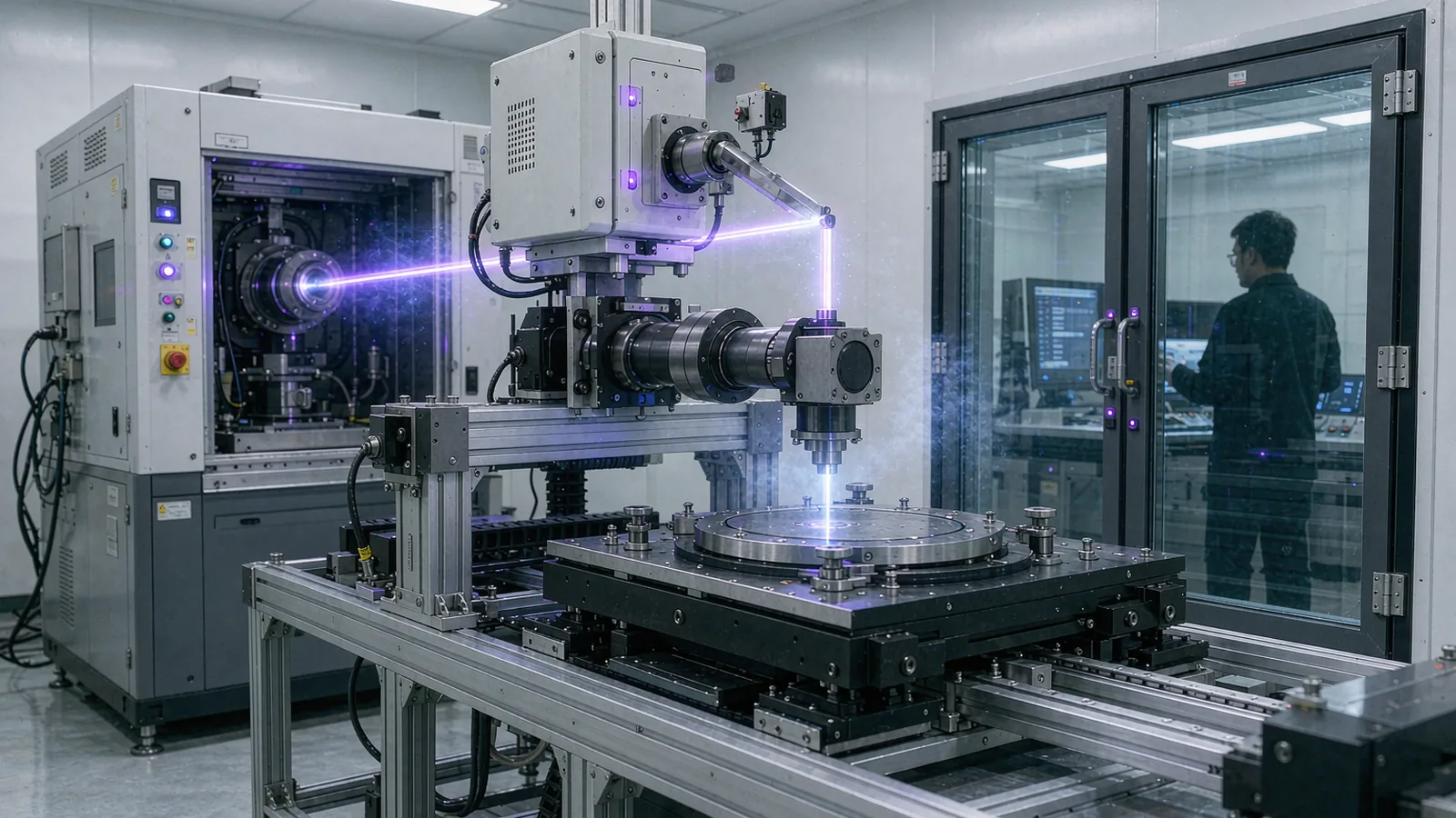
Laser direct imaging (LDI) is a digital exposure method that replaces the photomask with a modulated laser beam writing directly onto the substrate, dominant in PCB and flat-panel production. True maskless lithography for research and precision manufacturing is broader: scanning or digital exposure engines that write pattern data pixel by pixel or line by line, often with autofocusing, real-time alignment and grayscale capability on small substrates.
The two routes differ in exposure strategy, achievable feature size, throughput, mask logistics and cost of ownership. LDI optimizes large-area, high-throughput patterning at moderate resolution; maskless scanning systems optimize flexibility, fine features and low-volume, frequent-design-change work. The right choice follows substrate size, minimum feature, overlay requirement, design churn and annual volume, not the marketing label.
ENGINEERING CONTEXT
The terms "direct imaging", "direct write" and "maskless" overlap in supplier marketing, so buyers comparing quotation sheets frequently weigh tools that solve different problems. A system optimized to expose large panels quickly at 10-20 µm features is not interchangeable with a scanning lithography engine that holds sub-micron metrology on a 100 mm wafer. Choosing on throughput alone strands R&D groups with resolution they cannot use; choosing on resolution alone strands production lines with wafer-per-hour figures they cannot afford.
Discuss your requirement ↗CRITICAL REQUIREMENTS
Fix minimum feature, equal line/space, grayscale needs, substrate material and size, and whether exposure area must be stitched from multiple fields.
State layer-to-layer overlay targets, alignment mark types and whether alignment must run automatically per substrate or per field.
Define the real duty cycle: wafer or panel count per day, design change frequency, and write-versus-handling time split, so throughput quotes are comparable.
Compare capital, source lifetime and maintenance, software workflow, mask and reticle logistics avoided or incurred, and operator skill level.
BUYER MATRIX
Give every shortlisted supplier the same process definition and request configuration-specific proof.
| Attribute | Laser direct imaging (LDI) | Maskless scanning lithography |
|---|---|---|
| Primary domain | PCB, FPC, flat-panel and packaging panels at production volume | R&D, MEMS, micro-optics, semiconductor R&D and low-volume precision work |
| Exposure strategy | Multi-beam modulated writing, often large-area scanning with stage motion | Point, line or multi-beam scanning written from vector or bitmap pattern data |
| Typical resolution | About 8-20 µm features on production-class tools; finer on specialty systems | Down to sub-micron depending on wavelength, optics and stage metrology |
| Throughput driver | Panel size, beam count and data bandwidth | Write dose, field size, pixel count and stage speed; often minutes to tens of minutes per substrate |
| Mask handling | Eliminates photomasks for most layers; artwork changes are software | Eliminates masks entirely; every design is data, enabling same-day iteration |
| Cost profile | High capital but amortized over high volume; strong uptime economics | Lower volume per hour; cost dominated by write time, not consumables |
| Best fit | Stable designs at volume where mask elimination saves cycle time | Frequent design iteration, fine features, grayscale and multi-material research |
Mask-based projection lithography exists because a mask replicates a pattern with high throughput once it is made. LDI and maskless scanning lithography both attack the mask itself, but from different ends of the market. LDI emerged in printed-circuit-board and flat-panel production, where photomask cost and logistics for large panels had become a bottleneck for moderate-resolution work. It replaces the artwork film or mask with a digitally modulated multi-beam write head scanning across the panel, typically with stage scanning in one axis and beam deflection in the other.
Maskless scanning lithography for precision and research applications answers the same mask question at a different scale: small substrates, finer features, tighter overlay and more diverse processes. Here the exposure engine writes vector or bitmap pattern data directly, often wavelength-selectable (UV to 405 nm and below in some research tools), with autofocus and automated alignment between layers. The overlap in the middle of the market confuses buyers, which is why the comparison should start from the application's feature size, substrate and volume, not from tool categories.
Both routes remove mask procurement from the critical path, which changes the development workflow more than it changes any single spec. Design revisions that once waited days for a new mask become a file edit. This is often the decisive economic argument for R&D organizations, independent of either technology's raw throughput.
LDI write heads modulate multiple laser beams at high data rates to paint large areas quickly. The resolution ceiling follows from spot size, wavelength, beam count and the precision of stage synchronization, and production-class systems typically land in the 8-20 µm feature range, which is well matched to PCB and panel-level work. Dose uniformity is engineered across a large field, and data bandwidth becomes a real constraint: the pattern file for a large panel at fine pixel pitch is measured in terabytes, so RIP and data handling are part of the tool's engineering.
Maskless scanning systems for precision work trade area for finesse. A focused spot, often from a UV or violet diode source, writes vector-defined geometry with sub-micron positioning built on a metrology-grade stage with encoder feedback. Real-time autofocus maintains dose on non-ideal substrates, and some systems support grayscale exposure by modulating dose per pixel, enabling 3D resist profiles and micro-optics that a binary write head cannot produce. The stage's tracking accuracy and vibration environment then matter as much as the optics.
Buyers should therefore read resolution claims together with the exposure strategy behind them. A sub-micron claim with no stage metrology or autofocus specification is not comparable to one backed by published stage tracking accuracy and autofocus range. Ask for MTF or write-test micrographs on your resist and substrate, not only supplier benchmark values.
Two tools claiming "0.5 µm resolution" may differ in depth of focus, dose latitude, resist sensitivity assumed, and whether the number is a line-edge definition or a half-pitch. Write these questions into the RFQ:
Throughput comparisons mislead more purchases than any other attribute because the brochure figures are measured on different duty cycles. LDI throughput scales with panel size, beam count and data bandwidth and is quoted in panels per hour at a stated feature size; production economics work because the design is stable and the tool runs shifts. Maskless scanning throughput scales with total exposed area, pixel pitch and dose; a research substrate may take minutes to tens of minutes, which is irrelevant if the real bottleneck is design iteration and process learning.
Build the throughput model from your actual year: number of designs, revisions per design, substrates per revision, substrate size and required feature size. A group exposing 2,000 substrates per year across 200 distinct layouts has a fundamentally different optimum from a line exposing 200,000 identical panels. The first group's cost of ownership is dominated by flexibility and iteration speed; the second group's is dominated by uptime, spare parts and throughput per square meter.
Also model the write-versus-handling split. Load time, alignment time, autofocus acquisition and substrate mapping can dominate at small substrate sizes, and some tools batch or cassette these operations while others are manual-load. A tool with 30 percent slower write speed but cassette handling and automated alignment can out-produce a nominally faster manual system in real operations.
Multi-layer work makes overlay a first-order criterion. LDI systems typically use camera-based registration to substrate fiducials with panel-scale correction, adequate for PCB-class layers. Maskless scanning tools for precision work add automated mark recognition, per-field alignment correction and, in advanced systems, in-situ focus and dose control. The buyer should specify overlay in the same terms the process will be judged: mean plus a multiple of standard deviation, measured with the actual process materials and layer stack.
Process integration differs too. LDI runs on photoresist chemistries and exposure energies familiar from panel production, with high-power sources and sometimes vacuum chucking of large flexible substrates. Maskless scanning systems must be qualified with the buyer's resist, substrate topography and thin-film stack: reflective or transparent substrates change autofocus behavior, and thick or contrasty films change dose latitude. Request a write trial on your materials before purchase; it is the single most predictive evaluation step.
Stage metrology underlies both. Whether a tool stitches fields, scans continuously or steps, the reported pattern fidelity depends on the encoder feedback and mechanical stability of the motion system during exposure. Buyers evaluating fine-geometry tools should treat the stage and its feedback as part of the lithography system, and evaluate position feedback and vibration isolation with the same rigor applied to the optics.
Choose LDI when substrate area is large, features are in the 8-20 µm class, designs are stable and volume is high enough to amortize the capital: PCB and FPC production, flat-panel and display patterning, advanced packaging substrates. Its mask elimination alone often pays back through shortened cycle time and removed mask logistics, and its throughput economics are proven in production.
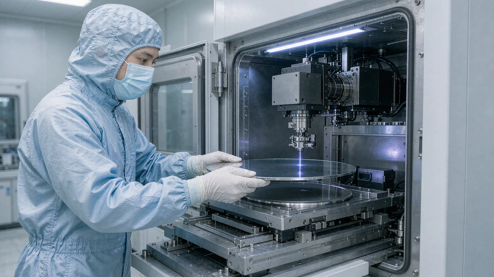
Choose maskless scanning lithography when design change frequency is high, features are fine, substrates are small, or grayscale and unusual materials are involved: MEMS, microfluidics, micro-optics, sensor prototyping, semiconductor R&D and university cleanrooms. Its economic strength is iteration speed and pattern flexibility rather than panels per hour.
SENFU's maskless laser lithography line spans this research-and-low-volume space: the ZML10A serves compact laboratory R&D, the ZML100A adds active autofocus and overlay for multi-layer work, and the ZML200A extends to substrates up to 8 inches. For teams whose path leads toward nanometer-scale e-beam work, the ZEL304G covers R&D electron-beam patterning. The correct shortlist starts from feature size, substrate, overlay and annual volume together, and SENFU application engineering can review those inputs against the exposure strategy each system actually provides.
CONCLUSION
LDI and maskless scanning lithography both remove the photomask, but they optimize different problems: LDI for large-area, stable-design, high-volume patterning, and maskless scanning for fine features, frequent iteration and research flexibility. Resolution claims, throughput figures and cost comparisons are only meaningful when the exposure strategy, stage metrology and duty cycle behind them are made explicit.
For a SENFU technical review, send the substrate material and size, minimum feature and grayscale targets, overlay requirements, design-change frequency and annual volume. SENFU can identify which lithography route and specific system configuration matches that profile, and arrange write trials on your actual materials before commitment.
SOLUTION ROUTES
EVIDENCE CHECKLIST
FAQ
LDI is a form of maskless exposure, but the terms are not interchangeable in practice. LDI refers to production-oriented direct imaging for large substrates such as PCB and flat panels at moderate resolution, while "maskless lithography" in precision and research contexts usually means scanning or digital exposure engines for finer features and smaller substrates. Compare tools by feature size, substrate and volume, not by label.
Production-class LDI typically resolves features in the 8-20 µm range on large panels; specialty systems go finer. Maskless scanning systems with UV sources and metrology-grade stages can reach sub-micron features depending on wavelength, optics and resist. Always verify the metric (half-pitch versus isolated line) and request write tests on your own materials.
For large panels at production volume, LDI is dramatically faster, often measured in panels per hour. Maskless scanning write time scales with area and pixel pitch and can take minutes to tens of minutes per substrate. Compare using your actual duty cycle: write time per substrate, handling, alignment and design-change frequency.
It matters most when designs change frequently. Every revision that would have required a new mask becomes a data file edit, cutting days to hours from each iteration. For stable high-volume production, mask elimination is still valuable for cycle time and logistics, but iteration speed is where maskless routes change the development economics.
Many maskless scanning systems modulate dose per pixel and support grayscale for 3D resist profiles and micro-optics, but capability varies in dose levels, linearity and calibration workflow. LDI is generally optimized for binary panel patterning. Request the grayscale specification and calibration procedure if 3D profiles are part of your process.
Send substrate material and sizes, minimum feature and line/space targets, grayscale needs, overlay requirements, design-change frequency, annual substrate count and cleanroom environment. SENFU can map those inputs to a specific system configuration, from compact ZML10A laboratory use to ZML200A 8-inch work, and arrange material write trials.
AUTHORITATIVE SOURCES
TECHNICAL REVIEW
Send the application, critical parameters and any drawing or process information available.
Discuss your application ↗