
Target profile
Define aperture, sag or relief height, lateral dimensions, slope, surface-quality metric and allowable profile deviation.
BUYER GUIDE / GRAYSCALE LITHOGRAPHY
Compare DMD grayscale lithography systems for micro-optics by profile, resist, substrate, calibration, overlay, metrology and supplier demo evidence.
Published
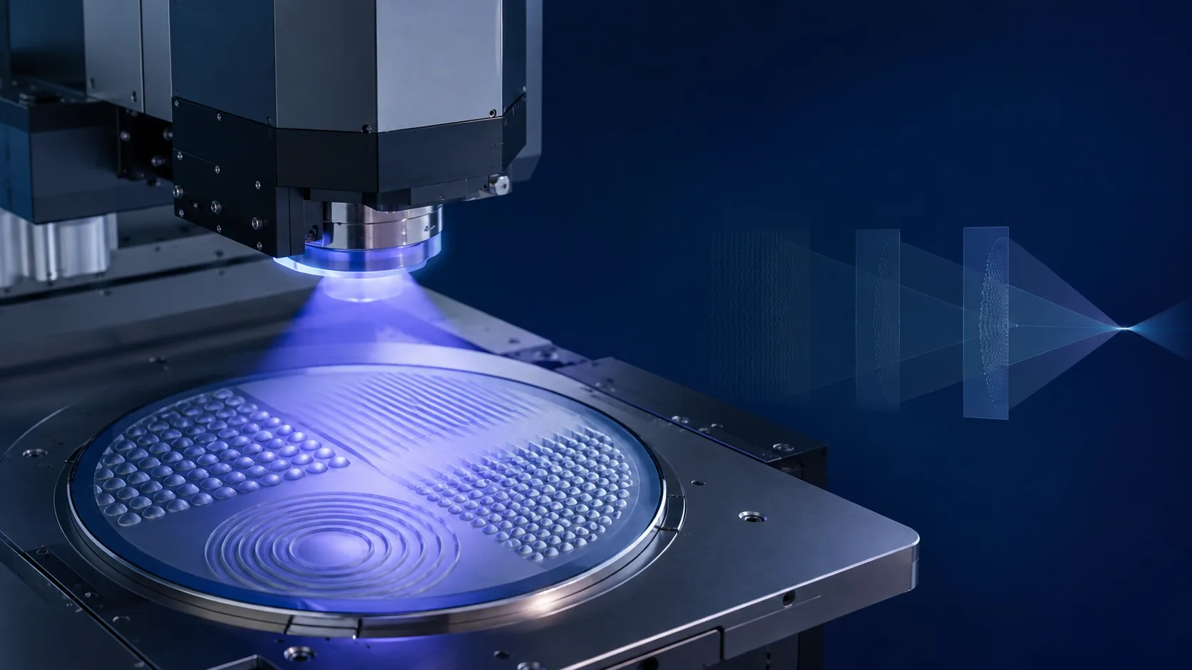
DIRECT ANSWER
Select a grayscale lithography system by the profile it can reproduce in your complete process, not by grayscale-bit count alone. A qualified comparison defines the target surface, lateral geometry, substrate, resist, exposure wavelength, development, profile metrology and any downstream etch or replication step. The supplier should then demonstrate a calibration method that maps digital input to measured resist height under those conditions.
For a purchasing decision, ask for a sample-based process trial, configuration-specific evidence and an acceptance plan. Evaluate focus strategy, field stitching, alignment, file preparation, recipe control and support alongside exposure capability. A strong request for quotation gives every supplier the same test vehicle and acceptance metrics, making technical fit and commercial risk easier to compare.
ENGINEERING CONTEXT
A system can support multi-level exposure yet still miss the required optical surface if the digital grayscale map, projected dose, photoresist response, development and profile transfer are not calibrated together. Buyers therefore need a process-qualified comparison rather than a headline feature comparison.
Discuss your requirement ↗CRITICAL REQUIREMENTS
Define aperture, sag or relief height, lateral dimensions, slope, surface-quality metric and allowable profile deviation.
Specify substrate, resist, film thickness, wavelength, bake, development and any etch, molding or replication step.
Agree on test patterns, sampling plan, profile metrology, repeatability runs, raw data and configuration control.
BUYER MATRIX
Give every shortlisted supplier the same process definition and request configuration-specific proof.
| Decision area | Define before the RFQ | Evidence to request |
|---|---|---|
| 3D profile | Target height map, aperture, sag, slope and tolerance | Measured target-versus-result profile data |
| Lateral pattern | Minimum geometry, pitch, edge and stitching needs | Micrographs and field-placement results with conditions |
| Process stack | Substrate, resist, thickness, bake, development and transfer | Recipe, calibration coupon and process-window data |
| Focus and alignment | Flatness, topography, layer count and overlay budget | Focus map, alignment method and repeatability result |
| Productivity | Pattern area, density, dose, objective and batch mix | Timed trial using the intended job class |
| Operations | File formats, recipe control, data retention and training | Workflow demonstration and document list |
A grayscale lithography system is part exposure tool, part process-development platform. It creates three-dimensional relief by varying local exposure dose so that development leaves different resist heights. For micro-lenses, diffractive optical elements, beam-shaping structures and other micro-optics, the commercial question is not simply whether a tool can display many digital levels. It is whether the configured tool and process can reproduce the required surface with usable repeatability.
That distinction matters because the final profile is created by several linked transformations. The design becomes a digital height or dose map; the projection optics convert that map into an aerial image; the resist converts dose into chemical change; development turns the latent image into topography; and an etch or replication step may transfer or scale that topography again. A weakness in any link can dominate the result.
NIST describes grayscale lithography as varying exposure intensity to produce resist thickness gradients and notes applications including digital lenses and MEMS. Recent DMD research also treats the aerial image, latent resist image and final contour as separate but connected modeling problems. For a buyer, this means process evidence should follow the complete chain from input file to measured functional surface.
Begin with a concise process specification that a supplier can test. Provide the intended optical function, but also translate it into manufacturing terms: clear aperture, height range, local slope, lateral feature size, pitch, edge transition, surface roughness metric and allowable profile error. A color image of the design is not enough; the evaluator needs a numerical height map or an equivalent geometry definition plus the acceptance method.
Separate the resist-master requirement from the finished component requirement. A resist profile may be used directly, transferred into glass or silicon, or replicated into another material. Each route changes what the lithography step must deliver. If downstream etching has a selectivity or loading effect, the target resist profile may deliberately differ from the final optical surface. State who owns that compensation and how it will be verified.
Height accuracy cannot be evaluated without lateral context. A calibration ramp, a dense lens array and an isolated freeform surface can respond differently because local image formation and resist behavior are not identical. Include representative pattern density, neighboring features and field boundaries in the trial vehicle instead of testing only one idealized element.
Record substrate material, size, thickness, flatness, reflectivity and surface preparation. Then define resist family, target film thickness, coating method, soft bake, exposure wavelength, post-exposure treatment if used, developer, time and agitation. If the process has not been fixed, ask the supplier to propose a development plan rather than present an unqualified performance promise.
Digital input, optical dose and developed depth are generally not one linear relationship. Peer-reviewed DMD work on arbitrary micro-optical surfaces reports nonlinear behavior between grayscale input and exposure dose as well as between dose and developed depth. The researchers used an empirical curve linking grayscale input to measured depth so the desired surface could be compensated before exposure.
A practical calibration therefore uses the intended resist stack and a defined optical configuration. Expose a coupon containing steps, ramps and representative curves; develop it with the agreed recipe; measure the topography; fit or tabulate the response; generate a compensated map; and repeat until the residual profile error is understood. When the resist lot, thickness, bake, wavelength, objective or developer changes, the calibration may need review.
Ask how calibration data are stored, versioned and attached to a production recipe. The operator should be able to identify which input transformation, exposure setting and process conditions produced a sample. For a multi-user research facility, recipe permissions and naming conventions can be as important as the initial result because they reduce accidental reuse of an obsolete curve.
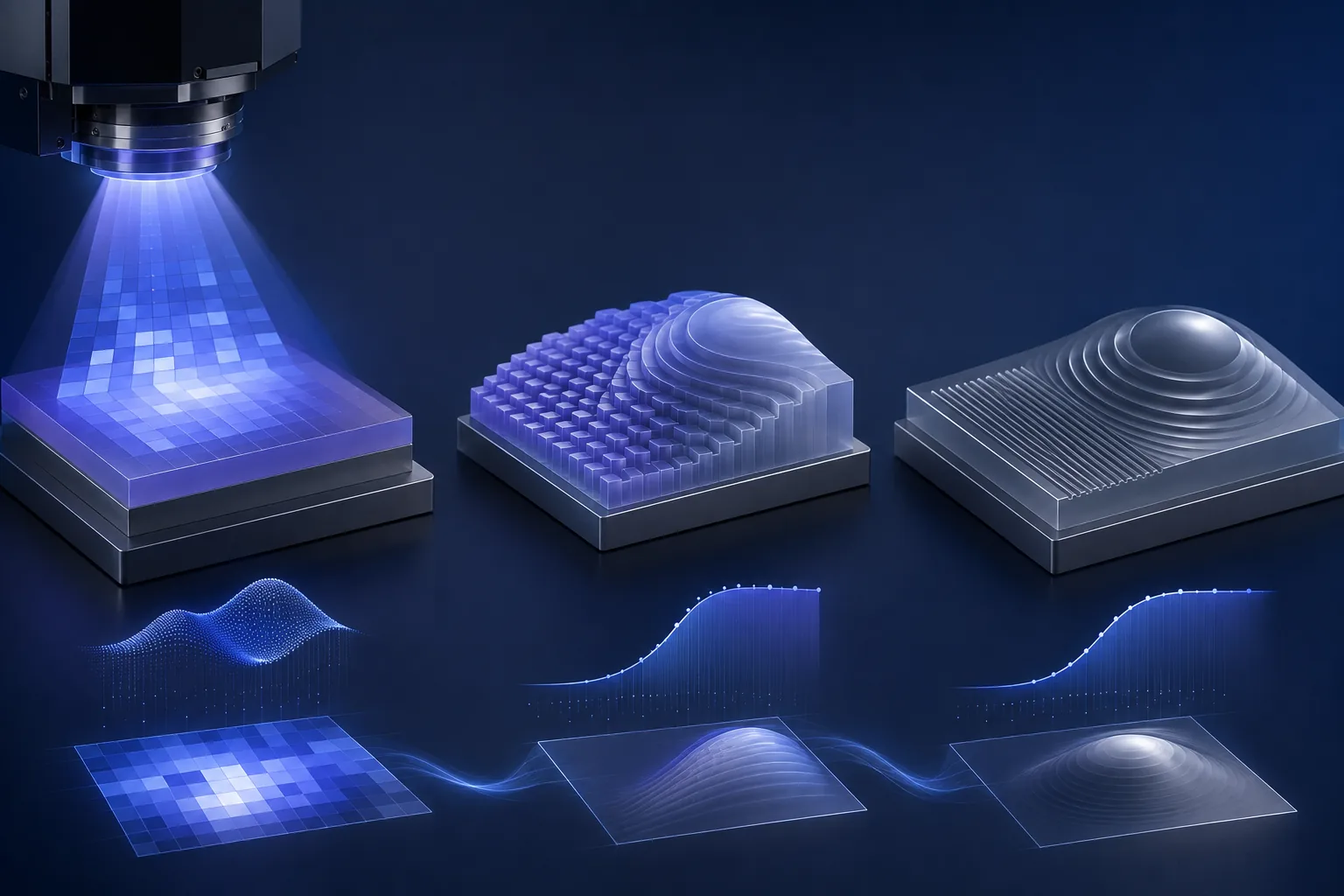
DMD grayscale performance depends on more than the micromirror array. Illumination uniformity, projection optics, objective choice, focus, stage motion and field strategy all influence the delivered dose distribution. During a supplier demonstration, keep the optical configuration fixed while establishing the baseline process. If several objectives or exposure modes are needed, qualify each as a separate recipe unless evidence supports a shared calibration.
For samples that are not perfectly flat, ask how focus is established across the exposure area and what the system does with tilt or known topography. Autofocus can support a repeatable workflow, but the buyer still needs to understand its measurement principle, valid surface conditions, scan strategy and relationship to the actual exposure plane. A feature name by itself does not define process capability.
Large patterns may span multiple projected fields, and multilayer devices may require alignment to existing marks. Put field boundaries and alignment structures into the evaluation design. Measure placement or profile continuity with the same metrology and sampling plan you expect to use after installation. For optical surfaces, a small discontinuity can matter even when a conventional binary line remains visually intact.
Exposure time varies with area, pattern density, dose, objective, focus actions, stage moves and data processing. Request a timed run using a representative file and include loading, alignment and any calibration checks that belong in the normal workflow. This produces a defensible capacity estimate without turning a best-case scan rate into an unsupported production claim.
A university nanofabrication facility, an OEM process-development lab and a pilot-production team may need different balances of flexibility, substrate capacity, automation and documentation. A compact platform can be appropriate when samples are small and recipes change often. A more automated platform becomes relevant when focus control, alignment, larger working area or repeatable operator handoff carries more value.
SENFU's ZML family is organized around different laboratory and substrate needs. ZML10A is positioned as a compact R&D platform and its documented configuration includes 2D and 8-bit grayscale capability. ZML100A adds active autofocus and advanced alignment functions, while ZML200A addresses projects requiring substrates up to 8 inches. These statements define comparison routes, not a guarantee for a particular profile; the final recommendation should follow a sample, recipe and evidence review.
Send the same evaluation package to each shortlisted supplier. Include a non-confidential representative height map, substrate and resist plan, target metrics, sampling locations and a list of required raw outputs. If the real design cannot be shared, create a surrogate coupon that preserves the difficult slopes, depth range, density, field boundary and alignment conditions.
Run the demonstration in stages. First, verify file import, coordinate conventions and data preparation. Second, expose a calibration coupon and review the measured response. Third, expose the compensated target. Fourth, repeat the target across locations or runs to examine variation. Finally, review how the recipe, calibration file, machine settings and results are packaged for transfer to the buyer.
Do not define acceptance with one attractive microscope image. Agree on the instrument, filtering, datum, profile registration, sampling density and calculation used for each metric. Fraunhofer research on grayscale process modeling emphasizes the value of measuring the full three-dimensional profile for calibration; the same principle makes a supplier trial more informative than a few selected line scans.
Technical success during a demonstration is only part of supplier qualification. Procurement and facility teams should request the configuration list, installation requirements, utilities, environmental limits, software and file workflow, preventive-maintenance scope, calibration procedure, training plan, service route and document revision method. Only accept certificates or compliance records that identify the covered model and scope.
Clarify ownership of process development. Determine whether the quotation includes a starting recipe, a completed sample trial, operator training, remote application support or only equipment delivery. Ask how future resist, substrate or profile changes will be handled and what information the supplier needs to reproduce a reported issue. These questions turn vague application support into a reviewable deliverable.
SENFU publishes source-backed product records and keeps model-specific documentation attached to the product it supports. Buyers can review the available resource registry, learn how the company handles claim scope on the about page, and use the contact form to request missing drawings, process evidence or a configuration review.
DMD grayscale lithography is attractive for flexible microscale relief and rapid digital design changes, but it should not be forced onto every feature. If a device combines broad three-dimensional micro-optics with critical nanoscale structures, a hybrid flow may reserve electron-beam lithography for the smallest geometry. NIST has demonstrated complementary photo and electron-beam grayscale processing for structures that combine large topography with fine detail.
The selection boundary should be written in the process plan: which layer creates the relief, which tool forms critical lateral features, how the layers align, and how metrology closes the handoff. Compare the cost and cycle time of the complete route, including coating, development, transfer and inspection, rather than comparing exposure tools in isolation.
CONCLUSION
The best grayscale lithography system is the one that can reproduce your required surface through a controlled, measurable and transferable process. Define the complete stack, qualify the calibration, measure the profile, test realistic field and alignment conditions, and keep configuration-specific evidence attached to the result.
For a useful SENFU review, send the target height map or representative coupon, substrate size and material, resist plan, lateral and vertical tolerances, patterned area, alignment needs, downstream transfer route and available metrology. Those inputs allow the discussion to move from a generic equipment comparison to a defensible evaluation plan.
SOLUTION ROUTES
EVIDENCE CHECKLIST
FAQ
Send a target height map or representative coupon, aperture and depth range, lateral geometry, substrate, resist and thickness, wavelength constraints, development plan, patterned area, alignment needs, downstream transfer step and acceptance metrology.
Bit depth alone does not establish profile capability. The useful result depends on how digital levels map to projected dose and developed height under the selected optical, resist and process conditions.
Use an agreed test vehicle and compare the measured three-dimensional surface with the target. Record the instrument, datum, filtering, registration, sampling and calculation, then repeat across relevant field positions or runs.
A change in resist, thickness, bake, wavelength, objective, developer or other material process condition can change the dose-to-height response. The calibration should be reviewed and requalified when a relevant condition changes.
Consider EBL when critical nanoscale lateral features or a specialized nanoscale 3D process drive the design. A hybrid route can use DMD exposure for broader microscale relief and EBL for the features that require it.
AUTHORITATIVE SOURCES
TECHNICAL REVIEW
Send the application, critical parameters and any drawing or process information available.
Discuss your application ↗