
Requirement defined before selection
Target linewidth and pitch, polarity of the pattern, required aspect ratio, downstream step (lift-off vs plasma etch), and acceptable write time per wafer, written down as the selection specification.
TECHNOLOGY / E-BEAM LITHOGRAPHY RESIST SELECTION
The resist is the component that turns an electron dose into a device geometry, and in electron-beam lithography it is chosen from a different set of materials than optical lithography uses. Sensitivity, contrast, etch resistance, and out-diffusion behavior interact with beam energy, dose strategy, and development chemistry in ways that determine linewidth, aspect ratio, and writing time. This guide compares the main resist families used in e-beam work, shows how the sensitivity-resolution-contrast triangle behaves in practice, and lays out a qualification workflow so resist selection becomes a documented engineering decision rather than an inherited habit.
Published
DIRECT ANSWER
Resist selection for electron-beam lithography is the choice of the polymer that converts a programmed dose distribution into a developed profile, and it dominates three outcomes at once: the smallest reliable feature and its edge quality, the aspect ratio the profile can hold, and the writing time per wafer, because dose and sensitivity set how many electrons each point needs. The main families are the classic positive polymethylmethacrylate (PMMA), high-contrast positive resists of the ZEP type, chemically amplified positive resists for sensitive, high-throughput work, and negative-tone inorganic resists such as hydrogen silsesquioxane (HSQ) for sub-10-nm lines and direct oxide etching.
No single resist wins. PMMA offers the highest resolution and clean lift-off but needs three to ten times the dose of ZEP-type resists; chemically amplified resists cut writing time dramatically but add bake-criticality and outgassing sensitivity; HSQ resolves atomic-scale features but demands careful handling and etch integration. Sound selection treats the resist as a component with a specification—resolution, contrast, sensitivity at the actual beam energy, bake window, developer, shelf life—and qualifies it on the own tool with a dose matrix and a contrast curve, exactly as any other critical subsystem would be qualified.
ENGINEERING CONTEXT
Most laboratories inherit their resist choice: a senior colleague used PMMA in IPA-MIBK a decade ago, the recipe lives in a lab notebook, and every new project starts from the same spin curve. The cost is invisible because it is distributed—longer writing times than necessary on routine patterns, lift-off scalloping or footing blamed on the process instead of the resist, and nanometer-scale work that quietly abandons targets because the incumbent resist ran out of resolution. The trap is that resist properties cannot be read from a datasheet in isolation. Sensitivity is specified for a given beam energy and developer; contrast is measured, not catalogued; resolution depends on pattern polarity, substrate, and development time as much as on the polymer itself. A team that selects resist the way it selects any precision component—requirement first, measured behavior on its own tool, documented qualification—gains linewidth margin, throughput, and a process that survives personnel changes. A team that treats resist as a consumable keeps paying the hidden tax on every exposure.
Discuss your requirement ↗CRITICAL REQUIREMENTS
Target linewidth and pitch, polarity of the pattern, required aspect ratio, downstream step (lift-off vs plasma etch), and acceptable write time per wafer, written down as the selection specification.
Dose-to-clear or dose-to-size measured on the actual tool at the actual acceleration voltage and development conditions, not quoted from a datasheet at a different energy.
A contrast curve (remaining thickness vs log dose), development-time window, and bake sensitivity measured for the chosen thickness and substrate, with tolerance limits recorded.
Shelf life and storage conditions, vial-to-vial consistency evidence or a re-qualification procedure for each new batch, and a second-source or frozen-stock strategy for long-running projects.
BUYER MATRIX
Give every shortlisted supplier the same process definition and request configuration-specific proof.
| Aspect | PMMA (positive) | ZEP-type (positive) | Chemically amplified (positive) | HSQ (negative) |
|---|---|---|---|---|
| Resolution | Highest in routine use; sub-10 nm demonstrated with thin films and suitable development | High; sub-15 nm practical with optimized process | Good but set more by acid diffusion length than by the polymer | Highest reported for dense features; few-nanometer lines demonstrated |
| Sensitivity / typical dose range | Low; roughly 200–1000 µC/cm² near 20–30 keV depending on film and development | Moderate; roughly 30–100 µC/cm² near 20–30 keV | High; roughly 5–30 µC/cm², the fastest writing option | Low to moderate; roughly 100–500 µC/cm² depending on energy and development |
| Etch resistance and integration | Poor plasma etch resistance; best for lift-off metallization | Moderate; usable for shallow etch and lift-off | Good etch resistance; industry-standard stack behavior | Etches like oxide; becomes the hard mask itself, ideal for direct etching |
| Watch-outs | Write time and thermal reflow above its glass transition; narrow development window | Scum in dense negative space, sensitivities to development endpoint; availability is single-source dependent | Acid diffusion blurs the intended dose gradient; bake timing and ambient control are process-critical; outgassing considerations in high-vacuum tools | Strict handling and storage discipline, moisture sensitivity, and a development (salt or TMAH) step that must be integrated with the substrate |
In optical lithography the resist absorbs photons from a uniformly flooded image; in electron-beam lithography the resist itself is the energy-stopping medium, and every electron that clears a feature has been delivered individually. That difference drives the selection criteria. The polymer must stop a useful fraction of the electron dose within the film thickness (which is why sensitivity is quoted in charge per area, not energy per area), it must convert that dose into a solubility change with as steep a transfer curve as possible, and it must survive the vacuum environment without outgassing material onto the column. The dose the resist demands is not a mere datasheet number: it multiplies directly into writing time, and at low doses the stochastic nature of electron arrival begins to roughen edges, a coupling between sensitivity and linewidth noise examined in the [shot noise and dose optimization guide](/technology/electron-beam-lithography-shot-noise-dose-optimization-guide/).
The second distinction is the transfer steepness, captured by the contrast number γ. High contrast turns a graded dose distribution into a steep sidewall and suppresses the energy spread the beam leaves in the resist; low contrast rounds profiles, widens lines, and makes proximity dose correction less effective because the resist response no longer acts as a threshold. Contrast is a measured property of the resist-developer-energy system, not a fixed polymer constant—development chemistry, temperature, and time move it substantially. This is why selection begins with the intended geometry: a dense line grating, an isolated nanowire, and a lift-off fence all rank sensitivity, contrast, and resolution differently.
PMMA remains the resolution reference of the field. A single-component polymer whose chains are cleaved by electron exposure, it develops in simple solvent mixtures and produces extremely clean, steep profiles with minimal scum, which is why lift-off metallization for nanogaps and quantum devices still defaults to it even at several times the dose of faster resists. Its liabilities mirror its virtues: low sensitivity means long writes, and its glass transition near 105 °C means ovens and hotplates must stay well below it or profiles reflow. ZEP-type resists—a copolymer of methyl α-chloroacrylate and α-methylstyrene—keep most of the resolution at roughly a third to a tenth of the dose, making them the pragmatic default for sub-50 nm positive-tone work where the write clock matters.
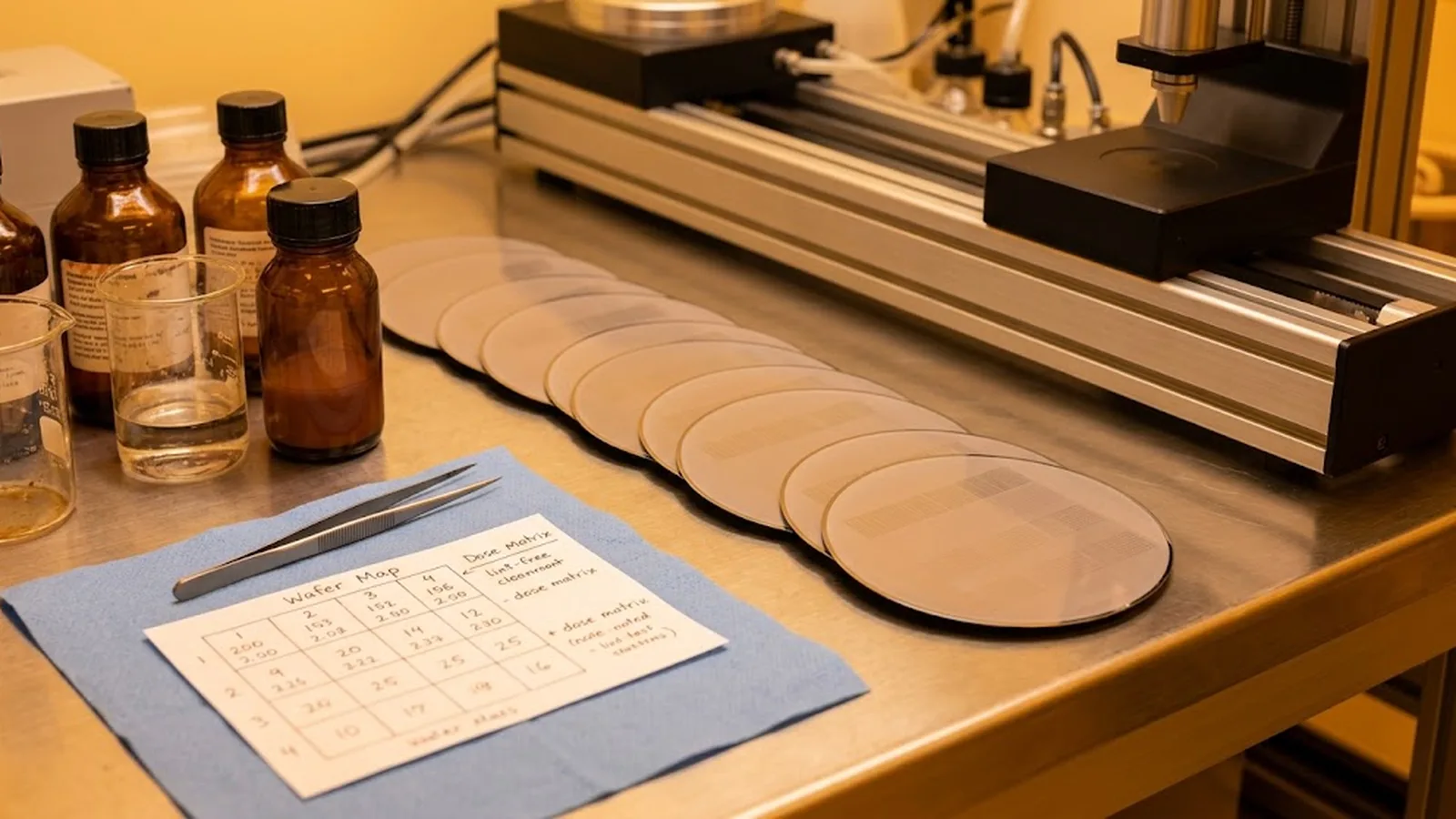
Chemically amplified resists import the acid-catalyzed deprotection chemistry of optical lithography: one exposure-generated acid unmasks many sites during the post-exposure bake, so doses of a few tens of µC/cm² suffice and throughput rises severalfold. The price is process criticality—bake temperature and time windows, ambient contamination control, and acid-diffusion blur that sets a floor on feature fidelity—and, in electron-beam tools, attention to resist outgassing during bake and exposure. HSQ occupies the negative-tone, inorganic niche: a network of silicon-oxygen cages that cross-links under irradiation, it resolves the densest features reported in the literature and, after exposure, etches as silicon dioxide, so it serves simultaneously as resist and hard mask. The detail image below shows the practical reality of selection: several candidate resists and developers on the bench, with the dose matrix and metrology samples that will decide among them.
The selection triangle is sensitivity, contrast, and resolution, and moving one corner moves the others. Raising sensitivity (lowering dose) buys writing speed but enlarges the stochastic linewidth spread and, in forward-scattering terms, lets more of the dose land outside the intended footprint; raising contrast sharpens profiles and narrows the effective linewidth but usually costs sensitivity; pushing resolution in thin films reduces etch depth and complicates lift-off because the film may be thinner than the metal stack it must template. The correct move is to budget the dose explicitly: estimate the write time from the pattern's total exposed area divided by dose-limited throughput, check the shot-noise margin for the smallest feature, and only then pick the resist whose sensitivity sits comfortably inside both constraints.
Sensitivity numbers must always be re-based to the operating condition. A resist specified at 100 keV on a membrane will demand several times that dose at 20 keV on a bulk silicon wafer, because backscattered electrons contribute dose the datasheet never saw; development chemistry shifts it again—undiluted developers raise sensitivity and lower contrast, mixtures do the reverse. The professional instrument is the contrast curve: a ladder of exposures at increasing dose, a thickness measurement of each field after fixed development, and a plot of remaining thickness against log dose whose slope yields γ. Two candidate resists compared by their measured curves on the production tool are comparable; two datasheet numbers quoted at different energies and developers are not.
A resist never acts alone. Coat thickness controls both resolution and aspect ratio—thin films resolve narrow lines but cannot hold high-aspect-ratio structures—while soft bake conditions set residual solvent and, in chemically amplified systems, the photoacid generator's initial state. Post-exposure bake is decisive for amplified resists: it drives the deprotection and simultaneously the diffusion that blurs the latent image, so the bake window is part of the resist's specification and must be held with the same discipline as any temperature-critical step in an optical process, as described for bake-driven overlay effects in direct-write practice. Development time and agitation define where the contrast curve actually lands, and endpoint decisions—clear or not clear—shift dose-to-size by tens of percent.
The resist's contrast also modulates how much proximity correction the pattern needs. A high-contrast resist approximates a threshold, so the dose map derived with the method in the [electron-beam proximity effect correction guide](/technology/electron-beam-lithography-proximity-effect-correction-guide/) translates directly into geometry and modest corrections suffice. A low-contrast resist integrates the surrounding dose, so dense-and-isolated bias grows and the correction tables must be re-derived for that specific resist and development. Practical selection therefore evaluates candidates on representative test patterns—dense gratings next to isolated lines next to large pads—because the interaction between backscatter dose and resist transfer curve is exactly what separates a resist that works from one that works in a datasheet.
Treat resist selection like any component qualification. First, write the requirement: critical dimension and tolerance, pitch, aspect ratio, polarity, downstream step, beam energy, and a write-time ceiling. Second, shortlist two or three families against the comparison above and the requirement. Third, qualify on the production tool: spin curves for the target thickness, a dose ladder at the operating energy, the contrast curve, and linewidth metrology at the qualified dose on a representative test pattern, recording line-edge roughness alongside mean linewidth. Fourth, freeze the recipe—thickness, bake temperatures and times, developer, time, temperature, and dose-to-size—and attach it to the batch record so every future vial re-enters the process through the same measured gate.
Batch-to-batch variation is the failure mode teams underestimate. Resist formulations age with storage, cold-chain interruptions change behavior, and suppliers revise chemistry; a frozen qualification for the wrong lot silently invalidates the dose. The defense is procedural rather than heroic: log lot numbers and storage history, run the short dose-to-size check on every new lot before production exposure, and keep the previous lot as a reference sample until the new one passes. Suppliers of electron-beam resists publish application notes and process-of-record documents—Kayaku Advanced Materials for PMMA families, Zeon for ZEP-type resists, Dow and successors for HSQ—and these belong in the qualification file next to the measured data, so the selection argument can be reconstructed years later. For laboratories that also run optical maskless exposure, the same requirement-first method applies across both tools, with the discipline described in the [maskless lithography resist processing window guide](/technology/maskless-lithography-resist-processing-window-guide/) serving as the shared framework.
CONCLUSION
In electron-beam lithography the resist decides, as much as the column or the stage, what the pattern will look like and how long it will take to write. Sensitivity sets the dose budget and with it throughput and shot-noise margin; contrast sets the transfer steepness that proximity correction and sidewall quality both depend on; resolution sets the floor the beam can aim at. The three corners trade against each other, and no datasheet resolves the trade—the production tool, at its own energy and with its own development chemistry, does.
The working method is compact: write the geometry and throughput requirement first, compare resist families against it, qualify the shortlist with dose matrices and contrast curves on the operating tool, and freeze the recipe under a batch-gated re-qualification procedure. A laboratory that runs this discipline gains linewidth margin, shorter writes, and a process that documents itself; one that inherits its resist recipe from an old notebook keeps discovering the same trade-offs, expensively, one project at a time.
SOLUTION ROUTES
EVIDENCE CHECKLIST
FAQ
Start with the pattern, not the resist. For lift-off metallization, nanogaps, and maximum resolution on thin films, PMMA in a standard IPA-MIBK development is still the cleanest and most forgiving entry point, and its high dose teaches the write-time cost early. For dense sub-50 nm positive-tone features where writing time matters, ZEP-type resists deliver most of the resolution at a fraction of the dose. Many laboratories qualify both and route patterns between them.
Usually, but not always. Lower dose raises the stochastic linewidth spread, so very sensitive resists may need their dose raised back up to meet linewidth noise requirements on the smallest features. Chemically amplified resists also add bake and ambient constraints that can cost more process time than the exposure saves. The honest comparison measures write time and resulting linewidth on the actual patterns.
The resist's contrast acts as a threshold on the deposited dose distribution, so correction tables derived for one resist-developer system do not transfer to another. High-contrast resists make the intended dose map reproduce faithfully in geometry; low-contrast resists integrate surrounding dose and widen the dense-versus-isolated bias. Any change of resist, development, or beam energy requires the proximity correction calibration to be re-run.
Occasionally, but with care. Broadband optical resists are formulated for photon absorption and usually demand large electron doses; some electron-beam resists lack the photosensitivity for optical exposure. Where a dual-use resist exists, the two processes still need separately qualified dose, bake, and development recipes, because the chemistry of image formation differs between the tools.
Keep the qualified lot as a running reference. On each new lot, coat a test wafer, run the short dose-to-size ladder for the critical feature, and compare the result and contrast slope against the frozen recipe's acceptance band before the lot enters production exposure. Log lot number and storage history either way. The check costs one wafer and an hour of metrology; an undetected lot shift costs a week of exposures.
AUTHORITATIVE SOURCES
TECHNICAL REVIEW
Send the application, critical parameters and any drawing or process information available.
Discuss your application ↗