Substrate envelope
Define material, size, thickness, bow, flatness, transparency, reflectivity and handling.
TECHNOLOGY / MASKLESS LITHOGRAPHY
Select a DMD maskless lithography system by matching substrate size, thickness, flatness, resist, wavelength, focus and inspection evidence.
Published
DIRECT ANSWER
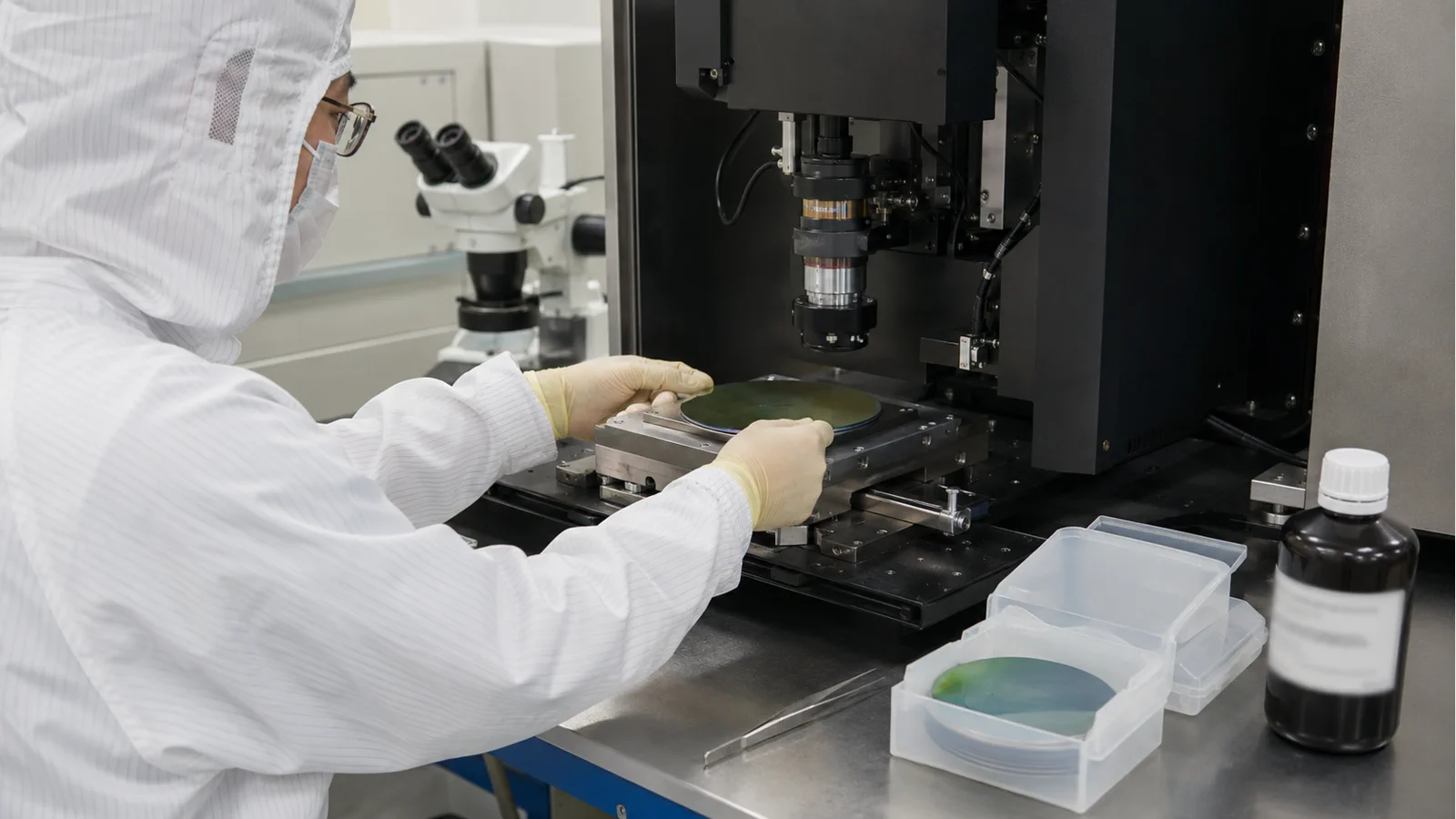
Match a maskless lithography system to the substrate and resist process before comparing resolution. Specify material, diameter or size, thickness, flatness, bow, transparency, surface reflectivity, resist type and thickness, exposure wavelength, dose, focus, alignment marks and inspection method. Then confirm the selected system's stage, objective, autofocus and file workflow for that combination.
SENFU documents ZML10A as a compact R&D platform with 385/405 nm exposure and sample formats up to 4 inches in the documented configuration; ZML100A adds active autofocus and motorized objective control; ZML200A is positioned for up to 8-inch substrates. These are system routes, not a blanket compatibility guarantee. A sample coupon under the buyer's resist and substrate is the evidence to request.
ENGINEERING CONTEXT
The same DMD optics can behave differently on glass, silicon, polymer, metal-coated or thick-resist samples. Focus, reflection, absorption, thermal load and handling can dominate the result, so the buyer must qualify a process window rather than only a tool headline.
Discuss your requirement ↗CRITICAL REQUIREMENTS
Define material, size, thickness, bow, flatness, transparency, reflectivity and handling.
State resist, thickness, bake, developer, dose window and downstream transfer.
Confirm wavelength, objective, focus, numerical aperture and feature geometry.
Require pattern, profile, overlay and throughput results on the real stack.
BUYER MATRIX
Give every shortlisted supplier the same process definition and request configuration-specific proof.
| Input | Evidence | Risk |
|---|---|---|
| Substrate | Size, thickness, bow, flatness and material | Stage or focus cannot handle the sample |
| Resist | Type, thickness, bake, dose and developer | Feature or profile is not transferable |
| Wavelength | Absorption and exposure condition | Dose window is too narrow |
| Focus | Autofocus or manual method on topography | CD and overlay drift across sample |
| Inspection | Optical/SEM profile and measurement rule | Tool result cannot be compared |
List material, diameter or rectangular size, thickness, bow, warp, flatness, transparency, reflectivity and edge exclusion. Include carriers, frames, fragments and bonded stacks. The largest and most difficult sample, not the average coupon, should drive the stage and objective review.
Handling is part of compatibility. State chuck or vacuum requirements, backside condition, particle limits, notch or orientation, load sequence and whether the sample can be touched. A system that exposes the pattern but cannot load or unload the production substrate is not compatible with the process.
Record resist family, thickness, bake, developer, post-exposure treatment and transfer step. Feature size and sidewall profile depend on the complete stack, not the optical image alone. Thick resists may need a different focus and dose window from thin films, while polymers or resists with strong absorption can change exposure latitude.
Include the process result that matters: line/space, opening, pillar, relief, grayscale level or etch mask. A vendor should demonstrate the selected stack or state clearly which part remains process development. Do not convert a result from another resist into an unsupported buyer guarantee.
ZML10A's documented 385/405 nm exposure options illustrate why wavelength belongs in the RFQ. Confirm the resist's sensitivity and substrate transmission or reflection at the selected wavelength. Ask for the objective, working distance, numerical aperture, field, focus range and any correction used for the actual pattern.
Optical compatibility is a process condition. The same layout can require different dose, focus or resolution when the wavelength or objective changes. Keep the selected wavelength and objective in the recipe and in the acceptance coupon so a later replacement does not change the process invisibly.
Flat silicon and a coated wafer do not present the same focus problem as a bonded microfluidic stack or a grayscale relief. Use the real surface, edge exclusion and mark layer in the focus test. ZML100A is documented with active autofocus and motorized objective control, which can be relevant when topography or thickness changes across the sample; the process still needs a measured focus window.
Map feature size or profile against focus at center and edge locations. Record warm-up, stage height, objective and substrate orientation. If manual focus is used, specify the operator sequence and repeatability. Focus evidence should be part of the supplier demo rather than an assumption made from the hardware list.
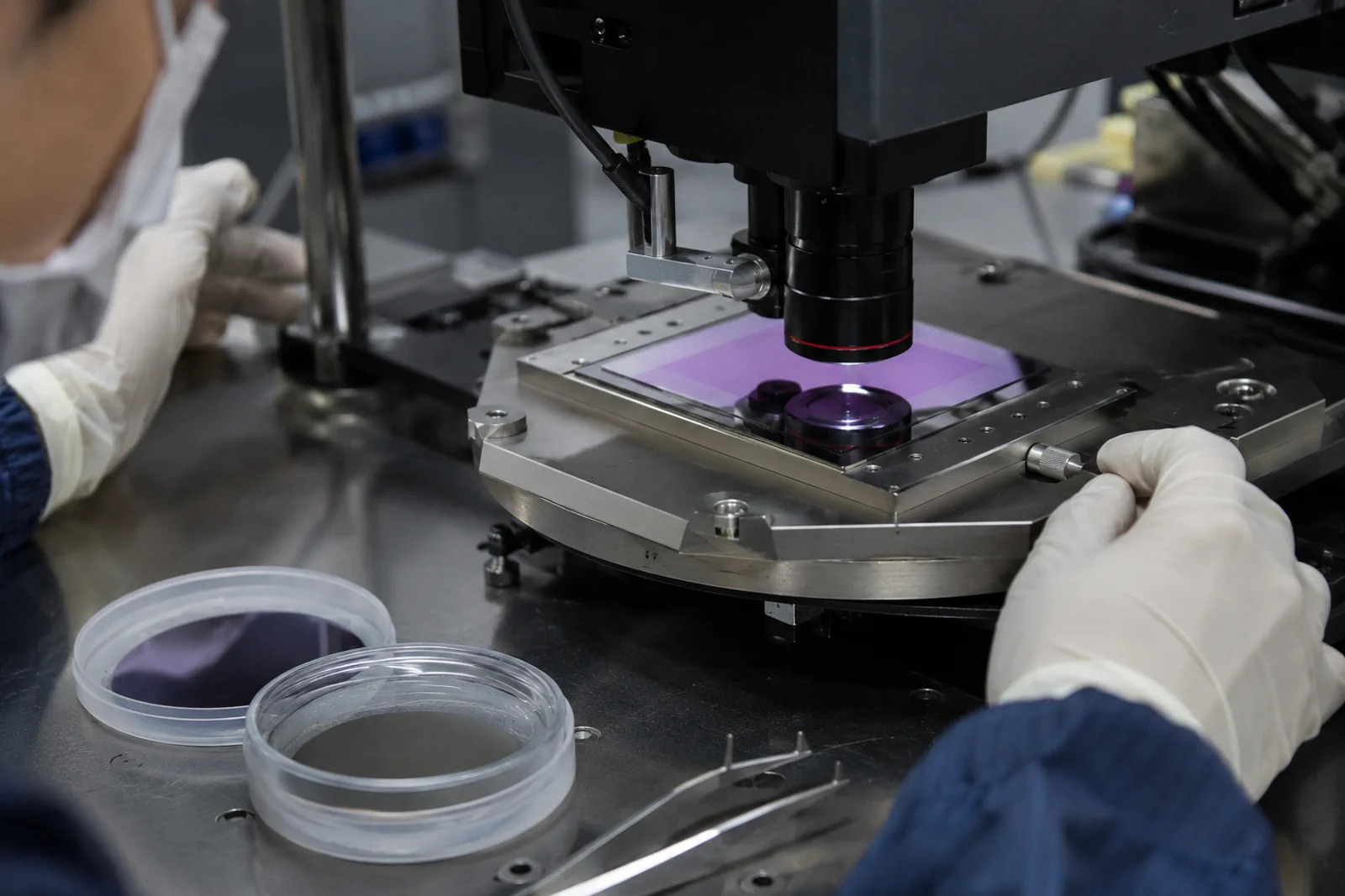
Define CAD format, scaling, orientation, layer names, alignment marks, coordinate origin and file conversion. The documented ZML workflow supports common direct-write formats, but the exact import and preprocessing should be confirmed for the intended system. A conversion that changes units or mirroring can create a process failure that looks like an optical error.
Use marks that survive coating and development and verify overlay with the same substrate and resist. If multiple tools are used, document the handoff coordinate and metrology. A compatibility review must include the file and alignment workflow, not only the optical head.
A good coupon includes isolated and dense features, openings, grayscale or relief elements and alignment marks. Measure CD, profile, sidewall or height, overlay and defects with the instrument the facility will use. Report dose, focus, wavelength, objective, substrate and resist with every result.
Throughput depends on area, pattern density, resolution, dose and focus strategy. Ask for time on the real substrate and pattern class rather than a maximum exposure rate. If a recipe requires repeated focus or alignment steps, include those operator minutes in the production estimate.
Specify cleaning, particle handling, stage materials, objective protection, resist fumes, exhaust and maintenance access. A DMD system may be in a laboratory rather than a fab, but the substrate and optics still need a controlled process. Ask which consumables and replacement parts are user-serviceable and which require a supplier visit.
Record how a change of objective, lamp or software is re-qualified. A new optical path can alter focus, dose and overlay. The buyer should have a clear recalibration and acceptance procedure before committing to the system.
Send the substrate matrix, resist stack, wavelength, objective, geometry, alignment marks, file format, inspection method, throughput case and environment. Request configuration-specific sample results and label guaranteed, typical and process-dependent values. Ask for drawings, recipe assumptions, software revision and a sample acceptance plan.
SENFU can compare ZML10A, ZML100A and ZML200A against the actual substrate and resist envelope and identify the coupon needed to close compatibility. The right choice is the tool that gives the facility a repeatable process window, not merely a platform with a suitable sample diameter.
A compatibility result should survive the normal variation of a research or pilot line. Repeat the coupon across the intended substrate supplier or lot, resist coating lot, operator and warm-up state. Keep the same file, orientation, chucking method, objective, focus routine and metrology. Report the spread in CD, profile, overlay and defects rather than only the best site. This is especially important for bonded or transparent stacks where thickness and reflection can vary across the sample.
Write the change-control rule before procurement. A new resist batch, substrate finish, objective, wavelength option or software revision should trigger a defined check, not an informal assumption that the recipe still works. Include consumables, cleaning and storage because contamination or a changed backside can alter focus and loading. A supplier who can explain the boundaries of the qualified window gives the buyer a more useful decision than one who supplies a single attractive micrograph.
Make the compatibility record easy to hand to the process owner. Store the sample drawing, recipe, focus map, metrology coordinates and photographs with the acceptance result, and state which values are measured on the buyer's equipment. When the pattern moves to etch, bonding or a second lithography tool, the same coordinate and material assumptions should remain visible. That continuity is what turns a direct-write demonstration into a usable manufacturing input.
CONCLUSION
Maskless lithography compatibility is set by substrate, resist, wavelength, focus, alignment, file workflow and metrology together. Qualify the real stack and report throughput with the same conditions.
SENFU can map the sample matrix to the ZML family and define a coupon and evidence pack before the tool is released for procurement.
SOLUTION ROUTES
EVIDENCE CHECKLIST
FAQ
No. It addresses sample envelope only. Resist, thickness, wavelength, focus, dose and handling still require process evidence.
Reflection and absorption change the exposure field and dose window. Test the actual material and coating rather than relying on a bare-silicon result.
It can help when topography, thickness or substrate variation changes focus, but the process should still demonstrate the focus window on the real stack.
Include critical and dense features, profile or grayscale structures, alignment marks, representative area, edges and a metrology plan.
Send substrate matrix, resist stack, wavelength, objective, geometry, alignment, file workflow, throughput and inspection method.
AUTHORITATIVE SOURCES
TECHNICAL REVIEW
Send the application, critical parameters and any drawing or process information available.
Discuss your application ↗