Functional budget
Translate overlay into coupling, pitch, gap, phase or optical-axis tolerance for each layer.
APPLICATION / PHOTONICS & MICRO-OPTICS
Plan overlay evidence for photonics and micro-optics by linking alignment marks, lithography tools, substrate handling and metrology uncertainty.
Published
DIRECT ANSWER
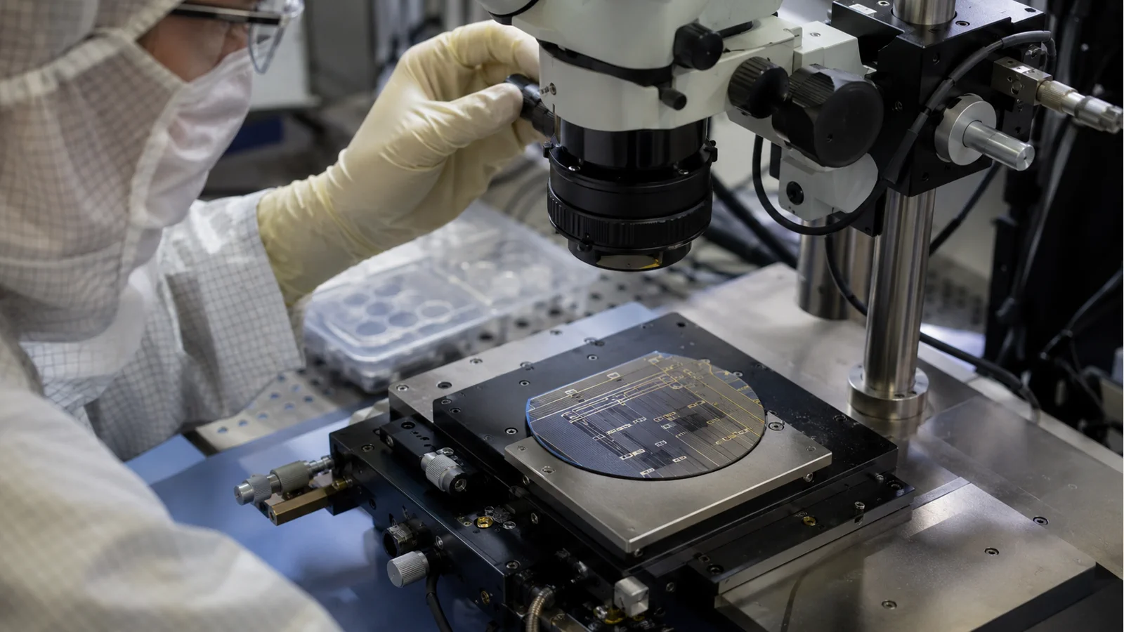
Photonics lithography overlay is only meaningful when the mark design, coordinate system, exposure tool, substrate handling and metrology method are specified together. Define the overlay budget by layer and by functional feature, place marks where the tool can see them, and measure the same wafer reference after each exposure. Report the result with substrate, resist, focus, alignment mode and measurement uncertainty.
Use DMD maskless or grayscale lithography for broad and profile-sensitive features and reserve electron-beam writing for critical nanoscale structures when the device needs it. ZML100A is documented with active autofocus, motorized objective control and overlay-oriented positioning; ZEL304G is documented for field calibration, stitching and multilayer exposure. Those functions still need a process coupon and an agreed metrology chain before they become a buyer claim.
ENGINEERING CONTEXT
Photonics devices often combine waveguides, gratings, couplers and relief profiles across several process layers. Overlay errors can come from marks, wafer handling, thermal drift, tool coordinates or the microscope measurement itself, so the buyer must qualify the chain rather than a single machine number.
Discuss your requirement ↗CRITICAL REQUIREMENTS
Translate overlay into coupling, pitch, gap, phase or optical-axis tolerance for each layer.
Select mark geometry, placement, contrast and protection for every tool and process step.
Define wafer datum, design transform, stage axes, focus and thermal state.
State instrument, sampling, uncertainty, operator method and data format.
BUYER MATRIX
Give every shortlisted supplier the same process definition and request configuration-specific proof.
| Layer question | Evidence | Risk |
|---|---|---|
| What must align? | Functional tolerance and layer-to-layer budget | A machine number is not tied to optical performance |
| Can marks be seen? | Mark design, contrast, location and process result | Alignment fails on actual resist or topography |
| What is the datum? | Wafer coordinate, chuck reference and transform | Overlay is measured in the wrong frame |
| What is measured? | Instrument, sampling and uncertainty | Metrology noise is reported as tool capability |
| Does it repeat? | Multiple wafers, fields and thermal states | A single best coupon hides drift |
Start from the photonic function. A grating coupler, waveguide crossing, lenslet, resonator or diffractive relief may tolerate a different lateral or rotational offset. Express the requirement at the device: gap, pitch, optical-axis displacement, phase error or coupling loss. Then allocate a budget to design, exposure, wafer handling, thermal movement and measurement. This avoids selecting a tool on a generic overlay figure that is not connected to the device.
Separate global translation, rotation, scale and local field distortion. A wafer may be globally aligned while a field stitch or local mark is wrong. Record whether the result is within one exposure field, across a stage move or between different systems. The budget should state which terms are calibrated and which must be demonstrated on a process wafer.
An alignment mark is a process feature, not just a CAD symbol. Choose geometry, depth, material contrast, size and protection so the selected objective or electron-beam system can detect it after coating, exposure, development, etch and cleaning. Place marks near the functional pattern and at multiple locations when local distortion matters. Document which layer owns the mark and how it survives the next step.
Test mark visibility with the real substrate and resist. A mark that is clear on bare silicon may be weak under a thick polymer or a grayscale relief. For multilayer photonics, keep a mark map and a naming convention that every tool and metrology station can interpret. This is a practical way to reduce alignment ambiguity when files move between teams.
DMD maskless lithography can expose flexible microscale layouts and grayscale profiles without a physical mask for every revision. ZML100A is positioned for workflows needing active autofocus, motorized objective control and tighter overlay handling. Grayscale lithography can be useful when a photonic element needs a continuous or stepped relief rather than a binary opening.
Electron-beam lithography is suited to critical nanoscale elements but writes serially and introduces field stitching, charging and throughput considerations. ZEL304G documents field calibration, stitching, overlay and multilayer automatic exposure functions. A hybrid process can assign broad profiles to optical direct write and critical features to EBL, provided the shared marks and metrology are qualified.
Overlay is measured in a coordinate system that changes when the wafer is loaded, rotated, clamped or thermally shifted. Define the wafer notch or flat, chuck reference, stage axes, origin, scale and any transform used by the exposure software. Record how the system locates the first layer and how subsequent layers inherit that coordinate. A clear transform makes it possible to diagnose whether an offset came from handling or exposure.
Use the same orientation and chucking procedure for development coupons and production wafers. If the process moves between tools, record mark handoff and rotation conventions. SEMI wafer-coordinate practices are useful background for keeping points unambiguous, but the facility should still define its own acceptance coordinate and data format.
A reported overlay is the difference between two measured features, so the microscope, stage, focus, image threshold, calibration and operator method contribute uncertainty. State the instrument, objective, pixel scale, sampling plan, fit method and repeat count. Separate repeatability from systematic transform error and keep the images or coordinate files that support the result.
Measure global and local terms. Use marks near corners, center and functional areas, and compare multiple fields or dies. For grayscale structures, measure both lateral registration and profile because an optical phase error may arise from height or sidewall variation rather than overlay alone. The measurement plan should be agreed before a supplier demonstration.
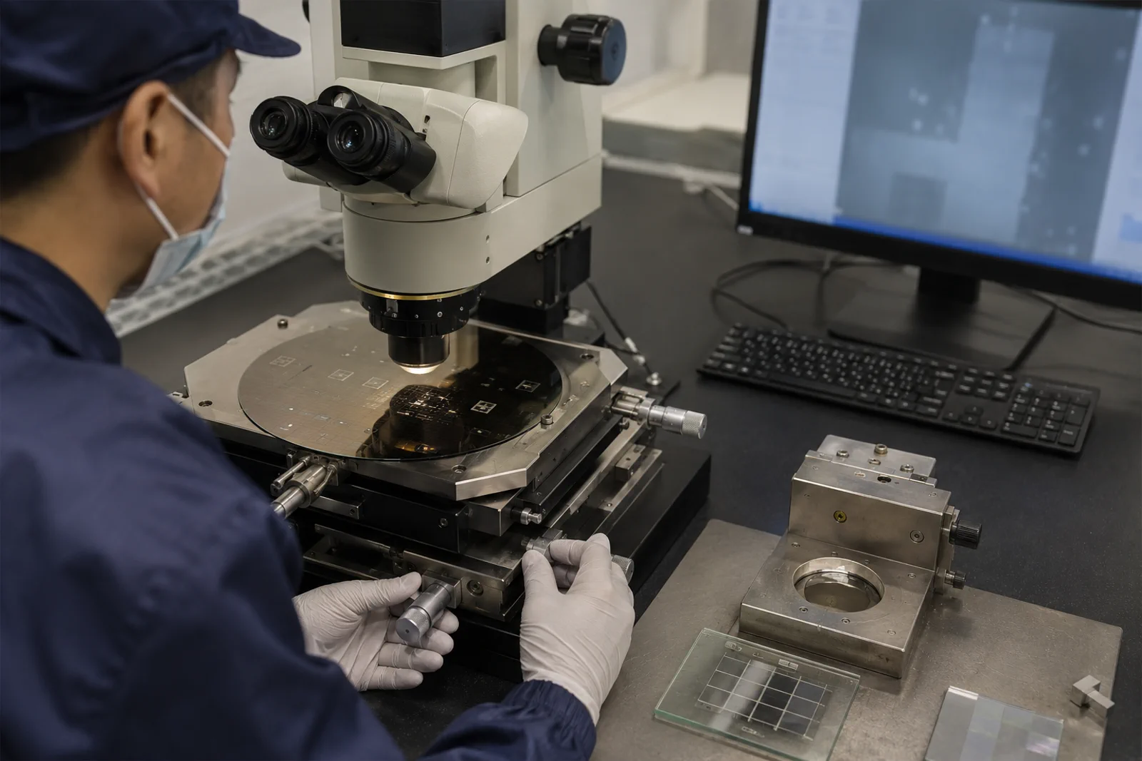
Photonics overlay can drift as the stage, chuck, objective and wafer reach temperature. Record warm-up time, substrate temperature, focus strategy and the time between alignment and exposure. Active autofocus can help maintain a focus condition, but the process still needs a measurement that shows how focus and topography affect the mark and feature coordinate.
Run a thermal sequence on a coupon with marks at several locations. Compare first exposure, steady state and restart after a pause. The goal is not to invent a universal drift number; it is to establish the conditions under which the tool's overlay evidence applies to the facility's process.
A supplier demonstration should use the substrate, resist, mark design, field size, layer count and inspection method the photonics team expects to use. Define the overlay statistic, number of sites, outlier treatment and whether the result is global, local or stitch-related. Ask for raw coordinate data and the tool and software revision, not only a marketing image.
Repeat the coupon after a reload, after thermal stabilization and across more than one field. If the workflow is hybrid, expose the same marks on both systems and measure the handoff. This creates evidence the team can carry into procurement, process transfer and future troubleshooting.
Send the supplier the device function, layer stack, mark layout, wafer format, resist and profile, exposure route, coordinate convention, thermal state and metrology method. Ask which claims are guaranteed, typical or process dependent and which are measured on a comparable coupon. Include the acceptance decision rule and data-retention requirement.
SENFU can review a photonics requirement across DMD, grayscale and electron-beam routes and identify where a documented system function needs a process demonstration. The best purchase decision is a complete measurement chain whose limits are visible to design, process, metrology and procurement teams.
CONCLUSION
Photonics overlay metrology connects device function, marks, wafer handling, exposure, thermal state and measurement uncertainty. Choose the route by feature and area, then prove the complete chain on the actual process stack.
SENFU can help compare ZML and ZEL routes, define a coupon and identify the evidence needed before a photonics tool is released to procurement.
SOLUTION ROUTES
EVIDENCE CHECKLIST
FAQ
Alignment is the tool action that places one layer relative to another; overlay is the measured result at the device or mark. The result also includes wafer handling, transforms and metrology uncertainty.
Grayscale exposure addresses profile control; overlay still depends on marks, stage, focus, thermal state and metrology. Treat profile and lateral registration as related but separate measurements.
Use EBL when critical nanoscale features or dense structures need it. Broader or relief-sensitive layers may be better suited to DMD or grayscale exposure, subject to a qualified hybrid alignment flow.
The number and placement depend on global transform, local distortion, field stitching and the device. Use enough sites to diagnose the error terms and agree the map before the demonstration.
Include substrate, resist, mark design, objective, focus, temperature, layer, site map, statistic, uncertainty, tool revision and raw coordinates or images.
AUTHORITATIVE SOURCES
TECHNICAL REVIEW
Send the application, critical parameters and any drawing or process information available.
Discuss your application ↗