
Optical target
Define phase, sag, slope, pitch, aperture, roughness and profile measurement method.
APPLICATION / MICRO-OPTICS
Build a grayscale lithography calibration plan for micro-optics by linking DMD dose levels, focus, resist, development and measured surface profile.
Published
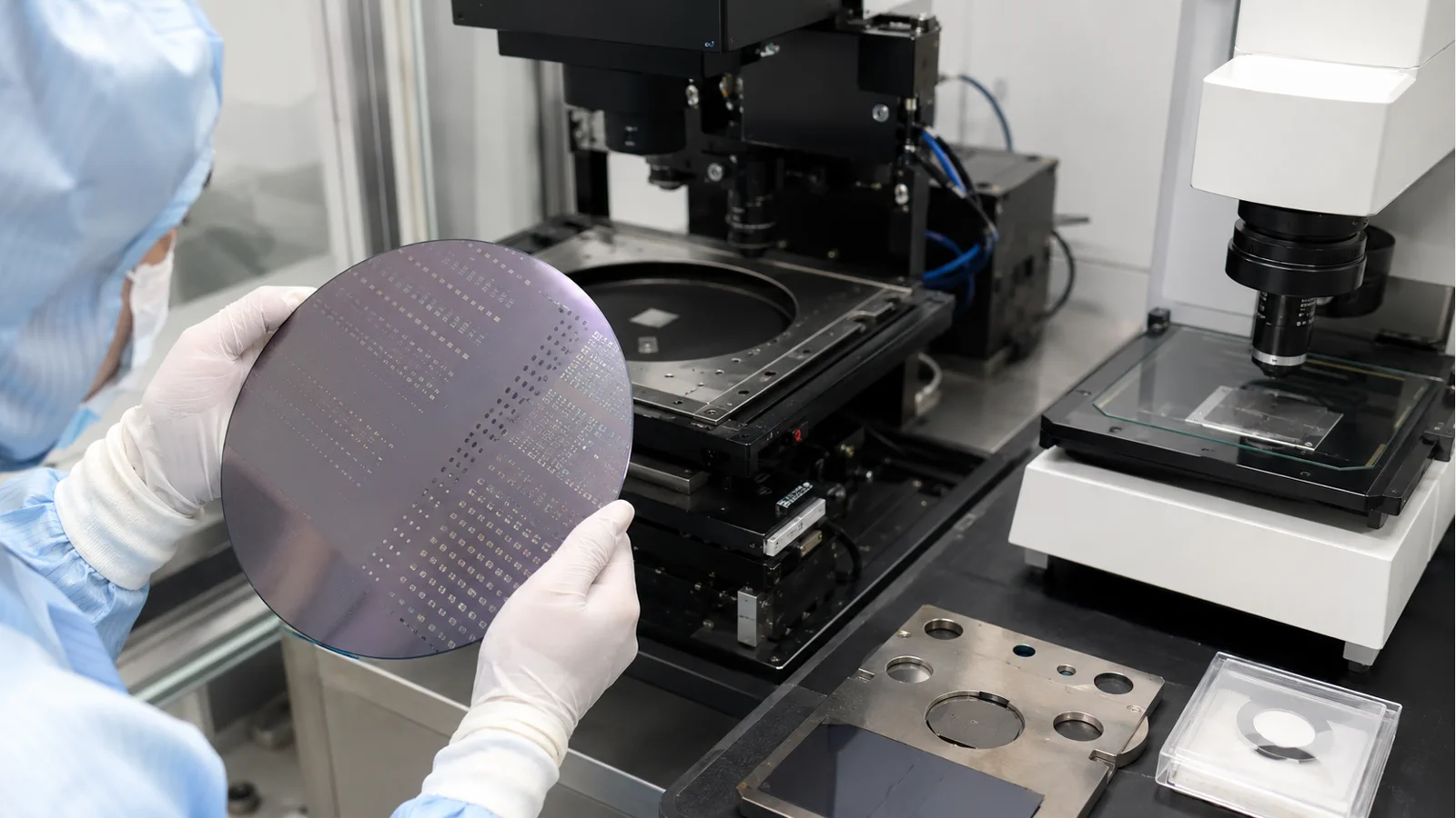
DIRECT ANSWER
Calibrate grayscale lithography by mapping the DMD exposure value and process conditions to a measured resist or etched profile. Define substrate, resist thickness, wavelength, dose encoding, focus, development, metrology, pitch, surface height and allowable variation. Build a dose-to-height or dose-to-depth table on the actual material and use it to generate the micro-optics design.
SENFU's grayscale lithography route is intended for profile-sensitive structures, but a platform capability is not a finished calibration. ZML100A is documented with active autofocus and motorized objective control, which can help stabilize optical conditions; the buyer must still demonstrate profile, uniformity, overlay and repeatability on the selected resist and substrate.
ENGINEERING CONTEXT
Micro-optics performance follows surface profile, not only a binary linewidth. Resist absorption, focus, dose quantization, development and etch transfer can all distort the intended lens, grating or diffuser, so calibration must be a measured process loop.
Discuss your requirement ↗CRITICAL REQUIREMENTS
Define phase, sag, slope, pitch, aperture, roughness and profile measurement method.
Specify material, thickness, absorption, bake, development and transfer.
Record wavelength, objective, focus, dose encoding and uniformity across the field.
Link design value to measured height/depth and repeat across the process window.
BUYER MATRIX
Give every shortlisted supplier the same process definition and request configuration-specific proof.
| Calibration term | Evidence | Risk |
|---|---|---|
| Dose encoding | DMD level or exposure value and repeatability | Design level is not proportional to profile |
| Focus | Focus sweep and topography result | Height varies across field |
| Development | Time, chemistry and endpoint | Profile rounds or collapses |
| Metrology | Profiler/AFM/optical method and uncertainty | Noise is mistaken for calibration |
| Transfer | Etch or mold transfer factor | Resist profile does not survive |
Start with what the micro-optic must do: phase delay, focal length, diffraction efficiency, beam spread or surface scatter. Convert that function into sag, height, slope, pitch, aperture and roughness requirements. A grayscale tool should be evaluated on the profile and optical response, not only on its pixel or line resolution.
Separate binary alignment features from the grayscale profile. The device may need marks, borders and support structures written with different exposure settings. Keep their metrology and calibration records separate so a profile result is not hidden by a good alignment image.
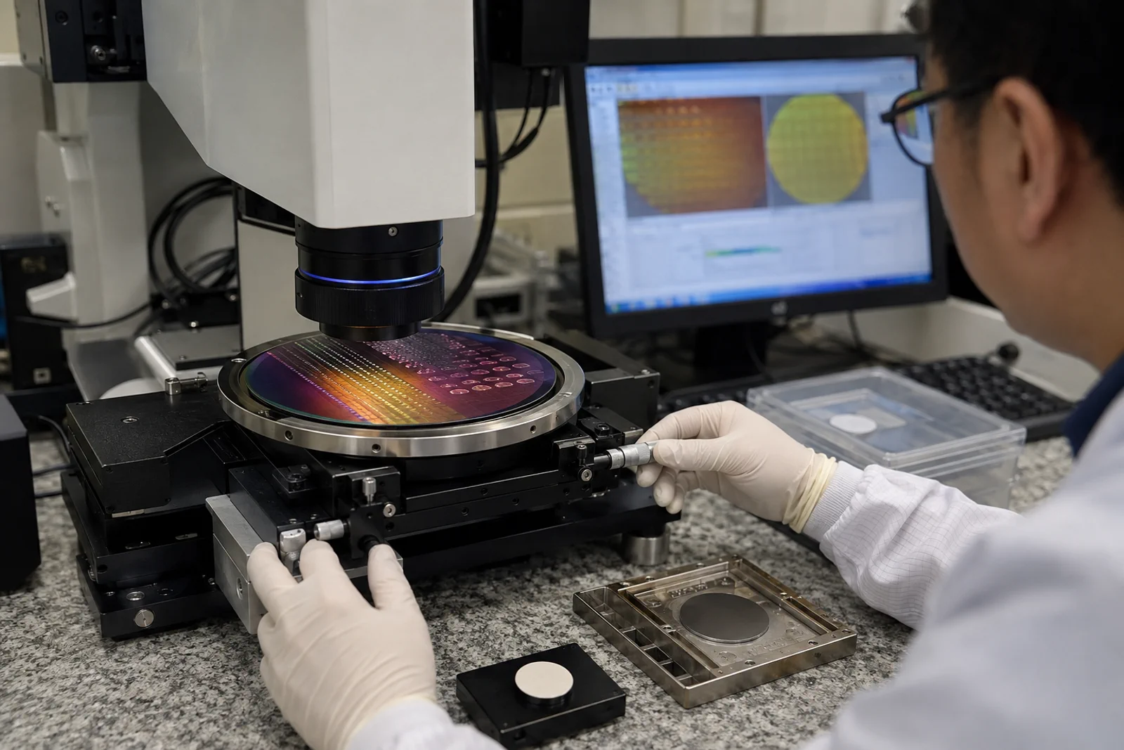
Expose a matrix of grayscale levels, line widths, pitches and pattern densities on the actual substrate and resist. Include center and edge sites and, when relevant, a focus sweep. Measure surface height or depth with the facility's profile instrument and record wavelength, objective, dose, bake and development.
The matrix becomes useful when the same process is repeated. Keep raw design levels, machine settings, metrology coordinates and fit method. Avoid assuming a linear relationship between exposure value and height; resist absorption and development can make the curve saturate or change with pattern density.
Resist thickness sets the available profile and the sensitivity to absorption. Specify material, thickness, bake, developer, wavelength and post-exposure handling. A calibration made on a thin film cannot be copied to a thick film or a different substrate without evidence.
Record coating uniformity and surface condition. Micro-optics often need smooth surfaces, but a resist edge or a substrate bow can change focus and profile. Include the process window that the facility can reproduce rather than selecting the most sensitive recipe from a single wafer.
Focus changes the aerial image and therefore the profile. ZML100A is documented with active autofocus and motorized objective control, which can support varying topography or sample height; the calibration should still measure profile across the field and after warm-up. Map focus, exposure and height at a defined grid.
Compare center-to-edge and die-to-die variation. If a profile is correct at the center but wrong near the edge, investigate stage height, objective, substrate bow, dose uniformity and design scaling. The calibration report should identify the conditions under which the profile table is valid.
Micro-optics may align to waveguides, electrodes, apertures or a second exposure. Use marks compatible with the resist and topography and measure lateral registration separately from height. Define wafer coordinate, rotation, scale and focus for each layer.
If the process combines DMD and EBL, reserve the critical layer for the route that can hold it and share a mark and metrology strategy. A beautiful grayscale profile is not useful if the optical axis is laterally displaced.
The resist profile may be an intermediate mask. Etch, reflow, deposition or molding can change height, slope and roughness. Measure the transfer factor on a representative material and include it in the design or calibration loop. Do not claim a final optical profile from resist data alone.
Keep a before-and-after record with process conditions and measurement uncertainty. If the transfer changes with aspect ratio or pattern density, add those features to the calibration matrix. This protects the buyer from a tool demo that stops before the step that determines optical performance.
Run the calibration on multiple wafers or days and record warm-up, operator, coating lot, dose, focus and development. Define the statistic—height error, slope error, RMS profile or optical response—and the site map. Keep outliers visible and document the reason for exclusion.
A useful acceptance coupon includes a functional micro-optic and a calibration matrix. The supplier should provide raw files, profile maps and recipe assumptions so the facility can repeat the test after installation or an objective change.
Provide optical target, substrate, resist, thickness, wavelength, objective, profile range, focus, alignment, transfer process, metrology and uniformity. Ask for calibration data with design level, exposure condition, measured height, field location and uncertainty. Mark which values are guaranteed or process dependent.
SENFU can review a grayscale micro-optics requirement against the documented lithography platforms and propose a calibration coupon. The decision should rest on a transferable profile process, not a generic grayscale label.
A dose-to-profile table is useful only when its assumptions travel with the design. Archive the raw grayscale levels, exposure file, wavelength, objective, focus map, substrate and resist lot, bake and developer conditions, metrology files and the fitted calibration curve. Record the usable range and the sites excluded from the fit. Keep a reference wafer or control structure so the facility can detect drift after an objective change, maintenance event or process transfer.
Use the calibration matrix to make design decisions explicit. Mark which levels are used for the lens, grating, diffuser or relief and where the process has insufficient slope or uniformity. If a resist profile is transferred by etch, molding or reflow, retain the transfer factor and repeat a final-material measurement. Procurement should receive the recipe boundary and requalification triggers, not just an image of a successful profile.
Include the optical consequence in the calibration review. A height error may change phase, focal length or diffraction efficiency even when the profile looks smooth, while a small lateral offset can move the optic away from a waveguide or aperture. Define the functional metric, the sampling locations and the acceptable uncertainty before selecting the dose table. This keeps the calibration tied to the micro-optic's job and makes later recipe updates auditable.
When several designs share one calibration, document the common assumptions and the exceptions. Pattern density, neighboring structures and edge proximity can change the local dose response, so retain the site map and any correction or exclusion rule. If the facility changes the substrate, resist thickness or developer, start a new calibration revision rather than silently editing the old table. That revision discipline helps engineering, procurement and the research team agree on which profile data is still valid.
CONCLUSION
Grayscale lithography for micro-optics is a measured dose-to-profile process. Control resist, focus, uniformity, alignment, transfer and metrology and retain the calibration conditions with the design.
SENFU can help define a profile coupon and compare the lithography configuration against the optical function and process window.
SOLUTION ROUTES
EVIDENCE CHECKLIST
FAQ
Not necessarily. Absorption, development, pattern density and transfer can make the dose-to-height relationship nonlinear, so measure a calibration matrix.
Use the instrument that measures the functional profile—optical profiler, AFM or another agreed method—and report scale, sampling and uncertainty.
No. It can help control focus, but uniformity must be measured across the field and under the real resist and substrate conditions.
Only with a transfer relationship. Etch or molding can change height and slope, so measure the final material.
Send optical target, substrate, resist, thickness, wavelength, objective, focus, alignment, transfer and metrology.
AUTHORITATIVE SOURCES
TECHNICAL REVIEW
Send the application, critical parameters and any drawing or process information available.
Discuss your application ↗