Mark strategy defined early
Alignment marks on the first side designed for visibility through the substrate or for reliable capture before flipping.
TECHNOLOGY / LITHOGRAPHY WORKFLOW
Double-sided devices require patterns on both substrate faces to register with each other, but the front side is often hidden once the backside process starts. This guide explains how backside alignment works in maskless lithography, which accuracy contributors matter, and how to specify and verify a double-sided workflow.
Published
DIRECT ANSWER
Backside alignment is the process of patterning one face of a substrate in registration with features on the opposite face. The system images alignment marks on the first-processed side—either through the substrate with an infrared-sensitive camera or by capturing and mirroring mark coordinates before the substrate is flipped—computes the coordinate transform between the two faces, and writes the backside layer relative to that transform.
In maskless lithography the same alignment hardware that supports front-to-front overlay can support double-sided work, but the workflow adds contributors: mark visibility through the substrate, substrate thickness and warpage, flip-induced coordinate rotation and mirror transformation, and chuck repeatability. Front-to-back overlay must therefore be budgeted and verified as its own metric, not assumed from front-side alignment performance alone.
ENGINEERING CONTEXT
MEMS inertial sensors, microfluidic through-holes, wafer-level packages and certain photonic devices all require features on both sides of a substrate to align within a few micrometers. The difficulty is physical: once the first side is processed, coated or metallized, its marks may be buried or invisible, and the operator must align to a face they can no longer see directly. Teams that treat backside alignment as an afterthought discover at device bring-up that vias miss bond pads, through-wafer interconnects short, and fluidic ports land off-channel—with no intermediate measurement to show where the process lost its registration.
Discuss your requirement ↗CRITICAL REQUIREMENTS
Alignment marks on the first side designed for visibility through the substrate or for reliable capture before flipping.
Material, thickness and backside coating evaluated for through-substrate imaging, or a mirrored-coordinate workflow specified instead.
Rotation, translation and mirror mapping between the two faces applied automatically, including wafer-to-chuck rotation.
A dedicated overlay verification across the substrate, using via openings, cross marks or IR inspection as evidence.
BUYER MATRIX
Give every shortlisted supplier the same process definition and request configuration-specific proof.
| Approach | How it works | Strengths | Watch-outs |
|---|---|---|---|
| Through-substrate camera | IR-capable camera images first-side marks through the transparent substrate in real time | Direct alignment to live marks; no memory of pre-flip position | Requires transparent substrate and IR contrast; thickness limits |
| Pre-flip capture and mirror | System captures mark coordinates before flipping, then mirrors and transforms them for the backside write | Works on opaque substrates; simple hardware | Depends on chuck re-clamping repeatability and stable flip reference |
| Fiducial in dedicated metrology step | Backside pattern registered to measured fiducial features written on the first side | Separates metrology from exposure; supports rework flows | Extra handling and measurement step; fiducial must survive processing |
| Manual microscope alignment | Operator aligns split-field microscope view of both faces before a masked exposure | No special software; familiar equipment | Operator-dependent accuracy; poor fit for maskless write workflows |
Many devices earn their function from what happens through the substrate. A MEMS accelerometer needs backside proof-mass cavities registered to front-side electrodes; a microfluidic chip needs ports drilled from the back to meet channels patterned on the front; through-silicon vias and wafer-level packages rely on interconnects that pass from face to face. In every case the two pattern levels live on opposite sides, and the registration between them is a device yield parameter as critical as linewidth.
Front-side overlay practice does not transfer automatically. After the first side is processed, its marks may be under metal, under deposited films or simply facing away from the alignment optics. The substrate may also have gained thickness, stress and warp from the first-side process stack. A double-sided plan therefore defines, before the first exposure, where the marks live, how they will be seen from the other side, and what overlay budget the second side must meet at every site.
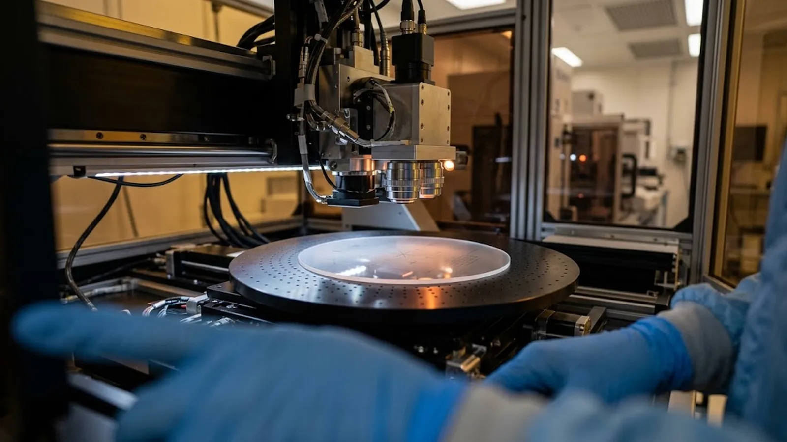
The through-substrate route uses an infrared-sensitive camera aligned to the projection path. For silicon and glass substrates, first-side marks are visible from the backside through the material; the system images them live, computes the substrate pose relative to the write coordinate system, and exposes the backside layer directly against what it sees. This is the most direct method because the alignment measurement and the exposure happen in the same reference frame.
The pre-flip route removes the transparency requirement. Before the substrate is turned over, the system captures the first-side mark coordinates; after flipping, software applies the mirror transform and any chuck-to-chuck rotation, and the write proceeds against the transformed map. Accuracy then depends on the mechanical repeatability of the flip and reclamp cycle, which is why the workflow should record and re-verify the transform rather than trusting a single calibration. In both routes, autofocus and focus control through the substrate thickness matter just as much as lateral alignment, because the write head must hold best focus on the second surface while compensating substrate wedge and warp.
Substrate properties lead the list. Thickness and material determine whether through-substrate imaging is possible and how much contrast the marks retain; IR transmission of silicon falls with doping and thickness, and backside metallization can block the view entirely. Warpage from first-side processing tilts and bows the substrate, displacing marks laterally at the focal plane and shifting focus across the field.
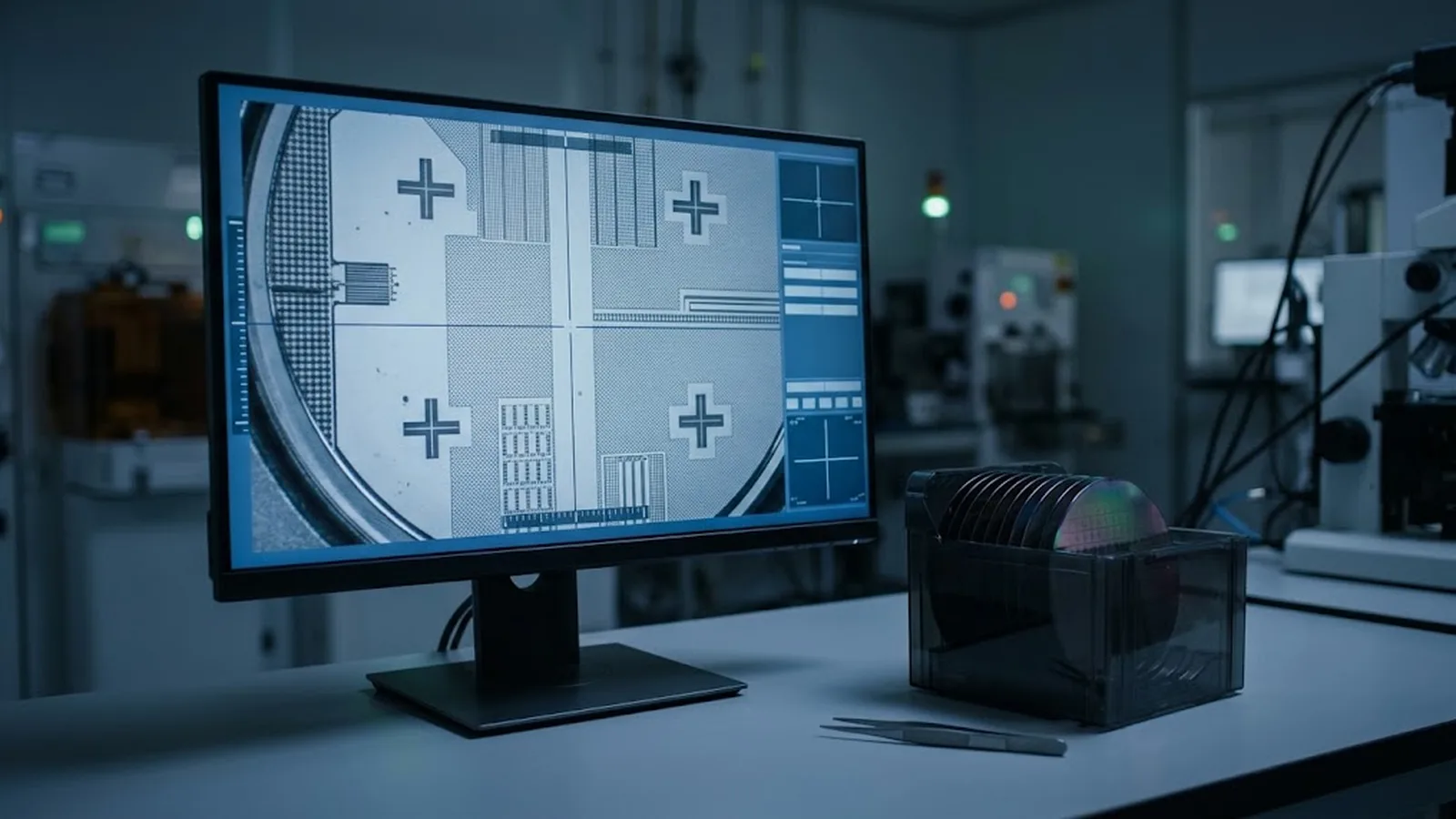
Mechanical and process contributors follow. Chuck clamping repeatability sets how faithfully the flipped substrate returns to a known pose; stage metrology and write-head synchronization define how accurately the transform is executed across the full exposure area; and mark degradation from the first-side process stack reduces the measurement quality of the very features the backside layer must align to. A verification pattern—via openings over buried targets, or cross-on-cross marks readable after development—turns these contributors into a measured front-to-back overlay number instead of an assumption.
Start the specification from the device: the overlay target, the substrate material and thickness range, the first-side process stack, and whether marks remain visible after processing. Then evaluate the tool against that list. Ask how the system handles the flip transform, what overlay performance it states for front-to-back work as distinct from front-to-front overlay, and which mark designs and contrast levels its alignment software expects. A supplier who documents these separately is describing a workflow they have run, not extrapolating from front-side numbers.
Verification belongs in the process, not after it. Write a dedicated overlay structure on the backside at multiple sites—center, edges, corners—registered to first-side targets, and measure it after development or after via etch. Record the overlay distribution, compare it against the device budget, and update the alignment recipe when the distribution shifts. SENFU supports double-sided workflows by documenting alignment capability, substrate handling and focus behavior per configuration, and an application review can map them to your device stack before committing a process.
CONCLUSION
Backside alignment extends lithography overlay to the face of the substrate the operator cannot see directly. Whether the system images marks through the substrate or carries a mirrored coordinate map across the flip, the same discipline applies: define the marks early, budget the flip and substrate contributors explicitly, and hold focus and pose as part of the alignment task.
Verify front-to-back overlay with dedicated structures at every qualification and re-verify it as the process stack evolves. Then both faces of the device register by design, and the through-substrate features that define the product land where the layout intended.
EVIDENCE CHECKLIST
FAQ
It is the alignment of a pattern on one substrate face to features on the opposite face. The system must locate first-side marks from the backside—by imaging through the substrate or by using coordinates captured before the substrate was flipped—and expose the backside layer relative to that reference.
Yes, with a pre-flip workflow: the system records first-side mark coordinates before the substrate is turned over, then applies the mirror and rotation transform for the backside exposure. Accuracy then depends on flip and reclamp repeatability, which should be measured and budgeted.
By writing dedicated verification structures on the backside that register to first-side targets, such as via openings over buried marks or cross-on-cross patterns, and measuring them optically after development or etch at multiple sites across the substrate.
Thickness, material and IR transmission determine mark visibility; silicon transmission drops with doping and thickness, and backside metallization can block the camera. Warpage and wedge from first-side processing shift marks laterally and move focus across the field.
Yes. A maskless system aligns and writes digitally, so the same alignment hardware and coordinate transform that support front-side overlay can support backside work when the mark strategy, substrate transparency and flip workflow are specified for it.
AUTHORITATIVE SOURCES
TECHNICAL REVIEW
Send the application, critical parameters and any drawing or process information available.
Discuss your application ↗