
Coating uniformity
Thickness control across the substrate, since a thickness spread directly becomes a dose-depth spread at the resist base.
TECHNOLOGY / MASKLESS LITHOGRAPHY
How absorption, dose depth and focus behave in thick photoresist, which exposure strategies produce straight high aspect ratio walls, and what development and bake conditions the structures need.
Published

DIRECT ANSWER
Structures above roughly ten micrometers of resist height stop behaving like thin-film lithography. Absorption in the resist makes the dose that reaches the bottom much smaller than the dose at the top, so a single blanket exposure tends to overexpose the surface while underexposing the base. Thick-resist work therefore relies on dose strategies—higher total dose, multi-pass writing with adjusted per-pass energy, or a dose ramp with depth—and on a focus position chosen for the structure's mid-plane rather than its surface.
Maskless direct write is well suited to this regime because the dose is set per exposure pixel rather than fixed by a chrome mask. High aspect ratio walls above 10:1 are routinely reached in chemically amplified epoxy resists such as SU-8 when coating thickness, exposure dose, post-exposure bake and development are tuned together. The practical constraints are coating uniformity over the substrate, the optical depth of focus relative to the resist depth, development transport inside deep channels, and stress cracking in very thick films.
ENGINEERING CONTEXT
A process window that is wide in thin resist becomes narrow in thick resist. The top of the film absorbs light first: raise the dose enough to crosslink the bottom of a hundred-micrometer layer and the top rounds out and closes; lower it and the base dissolves or peels during development. Focus adds a second variable, since the optical plane can only sit near the top or near the bottom, not both. On top of the optical problem, thick films bring mechanics—spin coating uniformity, bake gradients through the depth, capillary forces during development and tensile stress on drying. Getting tall, straight, repeatable walls means managing all of these as one process, not as separate steps.
Discuss your requirement ↗CRITICAL REQUIREMENTS
Thickness control across the substrate, since a thickness spread directly becomes a dose-depth spread at the resist base.
A light source whose wavelength and output power suit the resist chemistry and the film depth to be exposed.
Total dose, number of passes and per-pass dose adjustment chosen from measured exposure-matrix results, not from thin-resist datasheet values.
Post-exposure bake with controlled ramp, development agitation for deep structures and gentle drying to limit stress cracking.
BUYER MATRIX
Give every shortlisted supplier the same process definition and request configuration-specific proof.
| Aspect | Single-pass exposure | Multi-pass, dose-stepped | Multilayer coat and expose |
|---|---|---|---|
| Typical film depth | Up to a few tens of micrometers | Tens to hundreds of micrometers | Several hundred micrometers and above |
| Dose control | One total dose value | Per-pass dose adjusted by depth of penetration | Each layer exposed near its own surface |
| Wall verticality | Adequate for moderate aspect ratios | Improved base exposure, straighter lower walls | Layer interfaces may show steps |
| Process effort | Simplest, fastest | Exposure-matrix calibration per resist and thickness | Coat-expose cycles, alignment between layers |
| Typical use | Molds, fluidic channels of moderate depth | Deep channels, high aspect ratio MEMS structures | Very tall structures beyond single-coat limits |
In a thin film, dose variation through the depth is negligible and the exposure behaves as a two-dimensional problem. In a thick film, absorption attenuates the light as it travels, so the dose delivered at the base can be a fraction of the dose at the surface. The chemically amplified resists used for tall structures are formulated for high transparency, which extends the reachable depth, but the gradient never disappears and grows with thickness and with the absorptance of the formulation.
The consequence is a two-sided process window. The top of the film must not receive so much energy that features close or round, while the base must receive enough to crosslink fully enough to survive development. The usable overlap of these two conditions shrinks as the film gets deeper, which is why exposure dose for thick resist is always established experimentally on the actual thickness, using an exposure matrix rather than a datasheet starting point.
Focus behaves differently too. The optical plane of the writing tool sits at one depth, and features away from that plane are imaged with reduced contrast. For very deep structures, positioning the focal plane near the mid-depth or splitting the exposure across focal positions keeps the wall profile straighter than a surface-focused exposure.
The first lever is simply more dose, scaled from the datasheet value toward the energy the base of the film actually needs. The second and more powerful lever is writing in multiple passes with per-pass dose adjustment: an early pass at reduced energy avoids over-exposing the surface while later passes add energy that penetrates toward the base. Because a direct write tool controls dose per pixel in software, these ramps can be tuned without fabricating anything physical, and different regions of the same substrate can receive different strategies in one job.
In practice the parameters come from a calibration matrix: coat several tiles at the target thickness, expose each with a grid of dose and focus combinations, develop, and measure wall angle and residual base film. One well-executed matrix per resist-thickness combination pins down the working point; after that, run-to-run variation is handled with small dose trims validated by periodic cross-section checks.
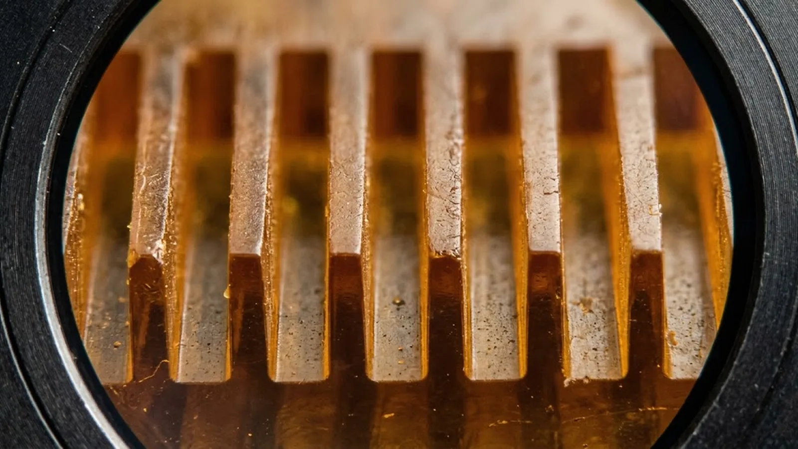
Exposure is only half of the process. The post-exposure bake must drive the crosslinking reaction through the full depth, and a controlled ramp avoids thermal gradients that set up stress between top and base. Development then has to remove unexposed resist from channels that may be hundreds of micrometers deep and a few micrometers wide; without agitation or solvent refresh, diffusion limits the rate and incompletely developed trenches leave residue at the base.
Stress is the third failure mode. Thick epoxy films shrink relative to the substrate and can crack on drying, especially over large exposed areas or sharp corners. gentler drying, baking schedules that relax stress, and layout choices—fillets, expansion slots, avoiding enormous solid areas—keep tall features intact. Aspect ratio limits are practical rather than absolute: walls above 10:1 are routine in well-controlled SU-8 processes, and even taller structures are reported with specialized support layers and critical-point drying.
Compared with a fixed chrome mask, direct write trades peak throughput for iteration speed and dose freedom. For mold masters, microfluidic prototypes and research structures where the layout changes or the dose strategy is still being tuned, the ability to rewrite in software and re-expose the same day is usually decisive. The pattern data is prepared at the target thickness, and grayscale or multi-pass capability lets the same tool serve both through-holes and tapered structures.
The equipment questions to settle before committing a thick-resist process are the optical depth of focus relative to the film, available exposure wavelength and power for the resist chemistry, substrate handling for heavy or oddly shaped carriers, and autofocus behavior on the coated surface. These are configuration-specific properties, so they should be confirmed with the actual resist stack and thickness in a feasibility exposure rather than inferred from general specifications.
SENFU treats thick resist as a system task that spans coating, exposure and development. The useful starting data are the resist and target thickness, the substrate size and shape, the minimum feature and aspect ratio, and the tolerance on wall verticality. With those, the exposure wavelength, dose strategy and focus concept can be defined and the feasibility questions settled against the actual process stack.
On the tool side, the relevant evidence is concrete: exposure dose range at the working wavelength, depth of focus for the chosen optics, autofocus behavior on resist surfaces, and demonstrated results on comparable thicknesses. Ask for a feasibility exposure on your resist and thickness so the process window is measured, not assumed.
Submit the structure requirement through the application form and SENFU can review it against the maskless lithography configuration and propose an exposure and calibration plan for the first process qualification.
CONCLUSION
Thick-resist lithography is governed by the dose gradient through the film: absorption, focus position and bake mechanics interact, and the process window narrows with every additional ten micrometers of height. Direct write gives the dose freedom—total dose, multi-pass ramps, region-specific strategies—needed to work inside that window without fabricating masks for each iteration.
Establish the window with an exposure matrix on the real thickness, verify walls by cross-section rather than top-down inspection, and control bake and development as carefully as the exposure itself. With those disciplines, high aspect ratio structures become a repeatable production result rather than a laboratory success.
EVIDENCE CHECKLIST
FAQ
Practice commonly treats films above roughly ten micrometers as thick resist, with chemically amplified epoxy resists reaching hundreds of micrometers in a single coat. The distinction matters because dose absorption and focus effects through the depth start to dominate the process window at these heights.
Aspect ratios above 10:1 are routine in well-controlled processes, and taller structures are reported with optimized coatings, exposure and drying methods. The practical limit depends on feature width, film depth, development transport and stress management rather than on the exposure tool alone.
Absorption attenuates the light as it passes through the film, so the base receives far less energy than the surface. A single increased dose often overexposes the top before the base clears. Multi-pass writing with dose stepping, or a dose ramp with depth, addresses the gradient directly.
For moderate depths, near the mid-plane of the film is a practical starting point because wall contrast at top and bottom balances. For deeper structures, splitting the exposure across focal positions can keep walls straighter. The best position comes from the exposure matrix, not from a general rule.
Control stress sources: ramp the post-exposure bake instead of stepping it, dry gently after development, avoid very large solid exposed areas, and add fillets or expansion features in the layout. Cracking risk grows with thickness and with stiffness mismatch to the substrate.
Send the resist system and target thickness, substrate size and material, minimum feature, aspect ratio and wall-angle tolerance, and the development capability available. SENFU can review the exposure configuration and propose a calibration and feasibility plan.
AUTHORITATIVE SOURCES
TECHNICAL REVIEW
Send the application, critical parameters and any drawing or process information available.
Discuss your application ↗