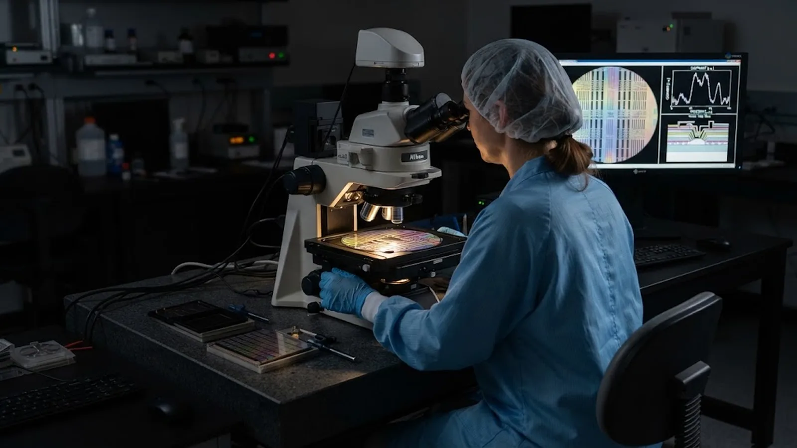
Wafer Alignment Mark Design for Maskless Lithography: Geometry, Signal Contrast, and Detection Reliability
Alignment marks are the fiducial contract between a wafer and its lithography tool, and their design decides whether overlay is measured cleanly or fought blind. This guide covers mark geometry options, how detection signal contrast is generated and lost, the process interactions that degrade marks layer by layer, and a design checklist that keeps marks detectable through the full process flow.
Published
DIRECT ANSWER
What should a buyer prioritize?
A wafer alignment mark is a deliberately engineered fiducial structure—etched gratings, boxed crosses, scribes, or today's grayscale-imaged dot patterns—that the lithography tool's alignment sensor must find with sub-micron repeatability before every exposure. Good mark design is a signal problem: the sensor extracts position from the contrast between the mark and its surroundings, so geometry, depth, material stack, and local topography jointly determine whether the returned signal has sharp, symmetric features or a washed-out smear. A mark that survives the process but returns weak contrast, or one that photographs beautifully but is destroyed by the first etch, both fail the same way—the tool misses, mis-centers, or reports low confidence, and overlay drifts without an obvious hardware fault.
The working rules are straightforward. Make marks large enough to be seen at the sensor's field of view but small enough to sit near the pattern they anchor, keep them symmetric so their signal centroid is unambiguous, put them on a stable layer with a defined depth rather than on film that changes during processing, and duplicate them—two marks per field minimum, four or more for critical layers—so a damaged mark is an anomaly, not a lost wafer. Then verify contrast on processed witness wafers at every step that touches the mark, because degradation is cumulative and usually silent.
ENGINEERING CONTEXT
The decision starts with the real constraint.
Overlay failures caused by mark design rarely look like mark problems. The tool reports an alignment error, operators recapture or lower thresholds, throughput drops, and sometimes wafers quietly process with degraded confidence because nothing is hard-failing. The root cause is usually decided months earlier, in the layout: a mark placed over dense topography that scatters the sensor beam, a shallow etch that thins out after a planarization step, a metal-covered mark whose reflectivity flipped sign relative to the design assumption, or asymmetric scribes whose signal centroid shifts with process bias. Maskless and direct-write tools raise the stakes further because many systems rely on alignment marks processed on the same tool, so a mark that only works with a stepper's specific illumination does not transfer. Teams inheriting third-party process flows frequently find that nobody owns the marks: the mask designer assumed the tool, the tool vendor assumed the process, and the integration engineer discovers the gap during overlay qualification, when every layer is already late.
Mark geometry only means something against a specific detection method—dark-field imaging, bright-field imaging, diffraction-based grating sensors, or grayscale pattern correlation. Design to the sensor's wavelength, spot size, and contrast mechanism, not to a generic drawing.
02
Process flow map for every layer touching the mark
Each film deposition, etch, polish, and clean between mark creation and final use changes the mark's optical signature. The design needs a written record of which layers cover the mark and by how much, so expected contrast can be predicted rather than discovered.
03
Witness wafer budget for contrast verification
Alignment contrast cannot be verified electrically. Plan processed witness wafers through the full flow, with mark contrast and signal symmetry measured after each major process step.
04
Placement and duplication plan
Marks must sit close enough to the pattern they anchor to control rotation and magnification, and far enough from active features to avoid process loading. At least two marks per exposure field, symmetrically placed, with defined spares for critical layers.
BUYER MATRIX
Compare evidence, not feature labels.
Give every shortlisted supplier the same process definition and request configuration-specific proof.
Alignment mark types for lithography detection compared
Aspect
Etched grating marks (diffraction sensors)
Boxed crosses / scribes (imaging sensors)
Grayscale / dot-pattern marks (direct-write correlation)
Signal mechanism
Diffracted orders from periodic structure; position from phase of the grating response
Optical contrast between mark edges and surrounding field; position from edge or centroid detection
Correlation of a gray-level pattern against the tool's stored reference; position from correlation peak
Strengths
Very high precision, robust to local defects, standard on steppers
Simple to draw and inspect, works with wide-field cameras and manual microscopy
No special mask layer needed, can be placed in pattern breaks, tunable contrast by gray level
Weaknesses
Sensitive to grating depth, film coverage, and process-induced period changes
Contrast collapses under reflective or planarized covers; asymmetry biases the centroid
Contrast depends on the imaging channel staying matched to qualification; pattern must resist process smearing
Best use
Production steppers and mix-and-match overlay between scanners
R&D, low-volume maskless work, backside and through-substrate alignment
Maskless direct-write tools exposing their own marks in-line with the pattern
What an alignment mark actually is: a signal generator, not a drawing
An alignment mark is best understood as a small optical instrument built into the wafer. Whatever the sensor technology, the measurement reduces to the same chain: the tool illuminates the mark, the mark's structure modifies the returned light—by diffraction, reflection, or gray-level pattern—and the detector converts that modification into a position estimate. Every property of the mark participates in the chain. Etch depth sets the phase contrast of a grating; line width sets which diffraction orders exist and how energy splits among them; the material stack sets reflectivity and its sign (metal on top versus metal underneath flips the perceived contrast); and the surrounding topography sets how much stray light contaminates the signal.
This framing explains most field failures that get mislabeled as tool problems. A mark that measures beautifully as a bare wafer can lose half its signal contrast under a conformal deposition, not because the structure changed but because the optical boundary conditions did. The design discipline, therefore, starts with the sensor's physics—wavelength, polarization, spot size, detection bandwidth—and works backward to geometry. Mark pitch is chosen relative to the illumination wavelength so diffracted orders land where the detector looks; mark depth is targeted at the quarter-wave condition for the process stack rather than at a nominal etch recipe; and mark width is kept well above the spot size so the signal has flat, symmetric plateaus instead of knife-edge features that amplify process bias. Overlay performance itself is a system property—the marks are the wafer-side input to a chain whose stage-side behavior is covered in the overlay accuracy fundamentals guide.
Geometry rules: symmetry, placement, and duplication
Symmetry is the first rule because nearly every sensor infers position from a centroid or a correlation peak, and asymmetry biases both. Grating marks should run uniform across their full length with clean terminations; boxed crosses should be geometrically symmetric about their anchor point; scribes used as alignment features should be checked for process bias that rounds one edge more than the other. A useful acceptance test is deliberately over-etching a witness wafer: a well-designed mark's reported position moves by only a few tens of nanometers, while an asymmetric mark can wander a quarter of a micron—directly into the overlay budget.
Placement is the second rule. Marks belong close to the pattern they anchor—typically inside or at the edge of each exposure field—because distant marks measure wafer rotation and magnification but let intra-field distortion pass unmeasured. At the same time they need clearance from dense features to avoid etch-loading differences that distort the mark itself. Duplication is the third rule: two marks per field define translation and rotation; four or more, symmetric about the field center, additionally expose magnification error and provide redundancy. A single lost mark should cost a capture retry, not a layer. For double-sided work, backside marks carry the same rules with the added complication that they are read through the substrate, which constrains substrate thickness and finish—the specifics are treated in the backside and double-sided alignment guide.
Mark degradation is cumulative and mostly silent, and it follows predictable mechanisms. Deposition layers thin the perceived edge contrast of imaging marks and shift the phase balance of grating marks; a metal cap can invert reflectivity so the detector sees the mark with reversed polarity, which some sensors tolerate and others silently mis-center on. Chemical-mechanical planarization is the classic killer—it removes the topography that imaging sensors depend on, leaving a flat wafer where the mark survives only as a residual material-contrast ghost. Etch processes round vertical edges and, with heavy loading, shrink the mark itself. Particles and resist residue sitting on the mark act exactly like contamination on an encoder scale: they add asymmetric scatter that biases the measured position, a parallel worth studying because the underlying optics are the same.
The countermeasure is evidence, not optimism. Build a witness-wafer sequence through the full process flow and measure signal amplitude and symmetry after every step that touches the mark, then set numeric release limits—commonly a minimum contrast ratio and a maximum asymmetry figure—so drift is caught at the process step that caused it. When a new film stack or a polish step is introduced, re-run the sequence before production, and record the resulting contrast as the new baseline. Teams that skip this usually discover the loss during overlay qualification, where it competes with stage error, resist effects, and thermal drift for attention; separating mark contribution early, using the metrology approach in the encoder-feedback overlay guide, keeps the diagnosis short.
Measure mark signal amplitude and symmetry after every deposition, etch, polish, and clean step on witness wafers
Set numeric release limits for contrast ratio and centroid asymmetry, not qualitative 'looks fine' judgments
Re-baseline after any film-stack, polish, or etch-recipe change before releasing the layer to production
Track per-site capture failures in production logs to catch site-specific placement or contamination issues
Maskless tools change the mark design calculus in two ways. First, they can write their own marks in-line with the pattern—grayscale dot fields or pattern-break fiducials—eliminating the dedicated mark mask layer but binding mark quality to the tool's own imaging channel and dose calibration; a mark written at a different effective dose than its qualification reference shifts its gray-level distribution and, with it, the correlation peak. Second, many maskless flows align once and then rely on the stage's optical encoders for the remainder of the exposure, so mark quality mainly sets the initial registration while stage metrology governs stitching and field-to-field placement. The two error sources must be budgeted separately or the mark gets blamed for stage error and vice versa.
Practical design practice for direct-write flows: write marks with the same dose calibration as the production pattern, qualify them on the exact resist and substrate stack in use, place them in pattern breaks or scribe regions where local topography is controlled, and keep their gray-level distribution well inside the sensor's dynamic range with margin for process-induced shifts. Verify the correlation signal's sharpness—peak width and side-lobe level—on witness wafers, because a broadened peak quietly trades repeatability for capture range. Finally, treat mark specification as a deliverable: geometry, stack, depth target, contrast limits, and verification sequence belong in the process documentation, so the next layer, the next tool, or the next engineer inherits a specification instead of an archaeology project.
Design the mark as a measurement, qualify it as a process.
Alignment marks are the wafer-side half of the overlay measurement, and they obey the same discipline as any precision sensor: contrast is designed in through geometry, depth, and material stack, and it is destroyed in predictable, measurable ways by the process steps that follow. Treating a mark as a drawing instead of a signal generator is what produces tools that miss, thresholds that creep, and overlay investigations that start in the wrong place.
The working method is compact: design to the sensor's physics with symmetry as the first constraint, duplicate and place marks to control the full field, verify contrast on witness wafers through every process step with numeric release limits, and re-baseline whenever the stack changes. A mark qualified this way stays a reliable fiducial for the life of the process—and when overlay does drift, the marks are the first thing the investigation can rule out rather than the last.
Alignment signal amplitude and symmetry measured on processed witness wafers after each layer that covers or etches the mark, compared against the as-created baseline
Mark detection repeatability (typically 3-sigma over 30 dynamic captures) recorded at qualification and after process changes
Signal centroid shift across a deliberately biased wafer—over-etch and under-etch splits—bounding the mark's process sensitivity
Capture rate and failure statistics per mark site from production logs, identifying any site-specific weakness
Documented correlation between alignment position and independent overlay metrology on the first articles of each new layer stack
FAQ
Questions engineers ask before selection.
How deep should an etched alignment mark be?
For diffraction-based sensors, the target is the depth that maximizes contrast between diffracted orders for the sensor wavelength and polarization—often near a quarter-wave optical path difference for the specific stack, which means the physical depth depends on the materials above and below the mark. Design to the optical condition for the full process stack, not to a fixed nm value, and verify on witness wafers after films are deposited, not on the bare etched wafer.
What causes an alignment mark to lose contrast after processing?
The main mechanisms are film deposition over the mark (thinning edge and phase contrast, sometimes inverting polarity), chemical-mechanical planarization (removing the topography imaging sensors rely on), etch rounding and process loading (shrinking and blurring the structure), and particles or residue on the mark (adding asymmetric scatter that biases position). Each is cumulative, so contrast must be verified after every step that touches the mark.
How many alignment marks are needed per exposure field?
Two well-separated marks are the minimum to define translation and rotation. Four or more marks placed symmetrically about the field center additionally expose magnification and some distortion errors, and they provide redundancy so a single damaged or contaminated mark costs a retry instead of a lost layer. Critical layers should carry spare mark sites by design.
Can maskless lithography tools use marks written in the pattern itself?
Yes—grayscale or dot-pattern fiducials written in pattern breaks are a common maskless approach, avoiding a dedicated mark layer. The trade-off is that mark quality is tied to the tool's own imaging channel and dose calibration: marks must be written with the same dose state as their qualification reference, qualified on the exact resist and substrate stack, and re-qualified when dose, resist, or imaging parameters change.
How is alignment mark quality verified in production?
Through a combination of witness-wafer contrast measurements (amplitude and symmetry after each process step, against numeric release limits), dynamic capture repeatability tests on the tool (3-sigma over repeated captures), and first-article overlay metrology correlating the alignment result with independent measurements. Production logs of per-site capture failures catch site-specific contamination or placement problems early.