Feature and alignment targets
Minimum electrode width and pitch, marker geometry and the layer-to-layer alignment budget for gated or multilevel devices.
TECHNOLOGY / MASKLESS LITHOGRAPHY
Plan maskless lithography for quantum and 2D material devices: micron-scale electrodes, flake-safe processes, overlay, charging control and rapid design iteration.
Published
DIRECT ANSWER
Maskless lithography is a strong fit for quantum and 2D material device prototyping because device geometries change constantly, substrates are small and often non-standard, and the critical features—electrodes, gates, contacts and markers—are micron or sub-micron scale rather than nanometer scale. A digital direct-write system exposes a CAD layout straight onto resist-coated chips without a photomask, so a new electrode design can be exposed the same day it is drawn, which is exactly the iteration rhythm 2D material and quantum device research demands.
Plan the process around the flake, not the lithography tool. Choose resist and exposure wavelengths that leave the material unharmed, use alignment to optical markers because flakes cannot survive registration processing, control charging on insulating substrates such as sapphire or SiO₂, and define alignment accuracy, minimum feature and write-time expectations for a representative chip before committing to a platform.
ENGINEERING CONTEXT
Quantum and 2D material devices sit in an awkward gap between fabrication routes. Electron beam lithography resolves nanometer features but is slow and expensive for the micron-scale leads and gates most devices need, while mask-based photolithography requires a new mask for every geometry change and handles small, irregular chips poorly. Research teams need micron-to-sub-micron patterning, fast design iteration, gentle process conditions and reliable alignment to flakes—capabilities that determine which lithography route a laboratory should invest in.
Discuss your requirement ↗CRITICAL REQUIREMENTS
Minimum electrode width and pitch, marker geometry and the layer-to-layer alignment budget for gated or multilevel devices.
Exposure wavelength, resist chemistry, dose and development conditions that leave graphene, TMDs, nanowires or superconducting films unharmed.
Small pieces, odd sizes and insulating substrates handled without chucks, charging or focus penalties.
CAD-to-exposure workflow, write time per chip, layout revision handling and multi-layer alignment workflow.
BUYER MATRIX
Give every shortlisted supplier the same process definition and request configuration-specific proof.
| Route | Strengths for this workload | Limitations to plan around |
|---|---|---|
| Maskless optical direct write | Same-day layout iteration, micron to sub-micron features, no mask cost, handles small chips | Sub-100 nm features and extreme density remain out of reach |
| Electron beam lithography | Nanometer resolution for quantum dots and dense gates | Serial writing is slow; charging on insulators needs discharge layers; high cost per chip |
| Mask-based photolithography | High throughput once masks exist; mature resist ecosystem | Mask cost and lead time per revision; awkward for one-off chips and frequent redesigns |
| Hybrid EBL + maskless optical | EBL defines nanoscale elements; maskless optics add interconnects and pads quickly | Requires overlay budget and process coordination between tools |
Quantum and 2D material device development is defined by iteration. A typical cycle changes electrode geometry, gate overlap or contact spacing after almost every characterization run, and devices are made one chip or a few chips at a time on small substrates that often host individually exfoliated flakes. Mask-based photolithography was designed for the opposite regime: fixed designs, high wafer counts and amortized mask sets. Paying for a new mask per design revision dominates both cost and calendar time in a research setting.
Maskless optical lithography removes the mask from the loop entirely. The pattern lives in software, is exposed directly onto resist by a digitally addressed optical head, and can be modified between chips at no incremental tooling cost. Shared-facility descriptions of modern maskless aligners emphasize exactly this role: rapid prototyping for quantum devices built from 2D materials, semiconductors and nanowires, alongside MEMS, micro-optics and sensors, with minimum structure sizes around one micron and second-layer alignment in the hundreds-of-nanometers class. For the interconnects, bond pads and gates that make up most of a 2D device stack, that capability window matches the requirement almost perfectly.
The lithography process must end with a functional flake. Exposure wavelength matters because many 2D materials and organic layers absorb strongly in the near-UV; modern maskless systems offer dual wavelengths, commonly 405 nm and 375 nm, so photosensitive stacks can be exposed at the longer wavelength where absorption and damage are lower. Positive resists with mild developers, moderate doses and gentle bake schedules should be selected jointly with the material growth team, and every new stack deserves a witness exposure on sacrificial material before a valuable flake is committed.
Direct optical patterning can even skip resist altogether for some materials: research on direct laser writing shows local modification, oxidation or removal of semiconductor and dielectric thin films at the micron scale, an approach demonstrated on chalcogenide films and nanocrystal layers. That resist-free path is niche but useful where polymer residues would contaminate sensitive interfaces. For conventional flows, plan the full stack—adhesion layer, resist thickness matched to metal step coverage, developer chemistry and lift-off or etch—and record it as part of the device run sheet so lithography outcomes stay comparable across design revisions.
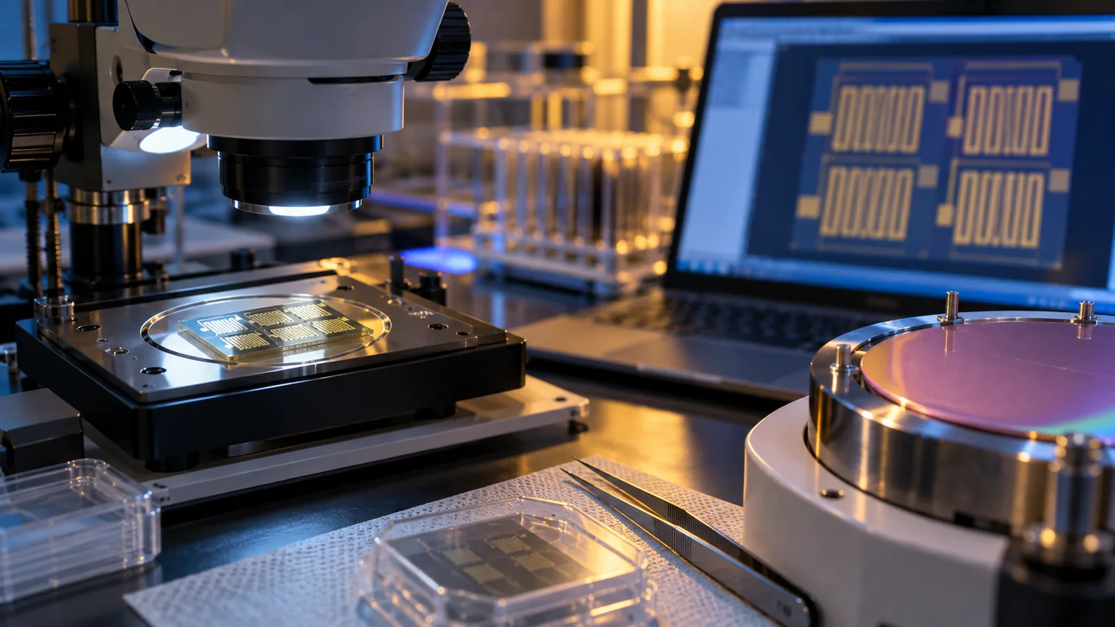
Multilevel 2D devices usually align the second lithography level to the physical flakes and first-level electrodes rather than to etched process marks. Optical alignment is therefore a core specification, not an afterthought. The tool must locate low-contrast markers—a metal edge, a gold pad, the flake itself imaged through transparent substrates—on small, often transparent or insulating chips. Maskless systems with through-the-lens or on-axis imaging handle this well because the same optics that expose the pattern also view the substrate.
Set the alignment budget honestly. Published maskless aligner data gives global second-layer alignment around 500 nm (3σ) and local alignment around 250 nm (3σ), which comfortably covers electrode-to-flake registration for most transport and optical devices. Devices that need sub-100 nm gate-to-channel registration still require electron beam lithography for that critical level, with the maskless tool providing leads and pads in a hybrid flow. Define which levels are critical and route each to the tool that meets its budget instead of forcing one technology to do everything.
2D material research rarely exposes full wafers. Chips are cleaved into pieces a few millimeters across, grown on sapphire, quartz or SiO₂, and carried individually. The lithography platform must hold small pieces without vacuum chuck damage, maintain focus across warped or uneven back sides, and expose to within a few millimeters of the piece edge. Confirm the minimum substrate size, thickness range and holding scheme for your formats before shortlisting a tool.
Insulating substrates also bring charging and focus behavior into scope. Optical exposure does not charge the substrate the way an electron beam does, which is a genuine advantage for sapphire and glass carriers; the remaining concerns are optical—substrate thickness affecting focus and backside reflections altering dose. A temperature-stabilized exposure environment helps resist uniformity across the small area. For quantum devices on piezoelectric or high-resistivity substrates, verify dose uniformity with a resist-based exposure matrix rather than trusting nominal settings.
Run these checks with your own chip formats during evaluation, because substrate handling issues appear only with real pieces in the holder.
Maskless optical exposure is area-based and fast by direct-write standards: published maskless aligner figures reach write speeds on the order of hundreds to over a thousand square millimeters per minute depending on wavelength, with a four-inch wafer exposed in minutes. A few-millimeter chip with sparse electrode patterns exposes in well under a minute of optical time, so the practical cycle is dominated by loading, alignment and development rather than writing. That cadence is what makes same-day design iteration realistic.
Contrast this with electron beam lithography, where serial writing makes even modest electrode layers a multi-hour session and insulating substrates need discharge layers to avoid charging artifacts. The review literature places direct optical lithography as the affordable micron-to-sub-µm complement to EBL for exactly this reason: it keeps nanoscale capability reserved for the few features that need it. Estimate your own write-time budget per design revision—area, density, alignment steps and development—and compare tools on a representative chip, not on vendor headline numbers.
Close the tool decision with a process demonstration on your own materials and formats. The demonstration should cover a representative electrode pattern at target linewidth, a two-level alignment structure measured against your budget, exposure of witness flakes or equivalent material to confirm process safety, and a full CAD-revision cycle from drawing to measured result to prove the iteration workflow end to end. Agree the acceptance criteria and metrology in advance so results are decidable.
SENFU supplies maskless lithography systems and the optical encoder metrology behind their stage accuracy, and supports exactly this evidence-first qualification flow for research cleanrooms. Send the device stack, feature sizes, alignment budget, substrate formats and target iteration cadence, and the team can review the fit against documented system capability before the laboratory commits.
CONCLUSION
Quantum and 2D material prototyping rewards laboratories that reserve each lithography technology for what it does best. Maskless optical direct write covers the micron-scale electrodes, gates, leads and pads that change with every design revision, at a speed and cost per iteration that masks and electron beam time cannot match. Electron beam lithography stays available for the sub-100 nm features that genuinely need it, ideally in a hybrid flow with a defined overlay budget between the two tools.
Qualify the route with your own materials: process safety on real flakes, alignment on real markers, substrate handling with real chip formats and a measured end-to-end revision cycle. SENFU can review the requirement against the maskless lithography platform and define the demonstration evidence needed before investment.
EVIDENCE CHECKLIST
FAQ
Yes, when the process is designed around the material. Longer exposure wavelengths such as 405 nm reduce absorption in 2D materials, mild resists and developers limit chemical attack, and witness exposures verify safety before valuable flakes are used. Many laboratories pattern graphene and TMD devices routinely with maskless optical systems.
Modern maskless aligners document minimum structure sizes around one micron with linewidth variation in the 100-nanometer class, which covers most electrodes, gates and interconnects in 2D and quantum devices. Smaller quantum-point contacts and dense gate arrays still need electron beam lithography for that level.
Through-the-lens or on-axis imaging locates the flakes, first-level electrodes or deposited markers optically, and the exposure is registered to those features. Published systems achieve global second-layer alignment around 500 nm (3σ) and local alignment around 250 nm (3σ), sufficient for most electrode-to-flake registration.
No. Optical exposure does not deposit charge the way an electron beam does, so sapphire, quartz and SiO₂ carriers avoid the discharge-layer requirement of electron beam work. Remaining substrate effects are optical—focus and dose uniformity—and should be verified with a resist-based exposure matrix on the actual material.
Because the pattern is digital, a revised layout can be exposed on the next chip without any mask-making step. Sparse electrode patterns on a few-millimeter chip expose in seconds of optical time; the practical cycle is set by loading, alignment, exposure and development, typically within the same day.
Send the device stack and materials, minimum feature and pitch, layer count and alignment budget, substrate materials and formats, expected chips per month and the iteration cadence you need. SENFU can review the requirement against the maskless lithography platform and propose the qualification demonstration.
AUTHORITATIVE SOURCES
TECHNICAL REVIEW
Send the application, critical parameters and any drawing or process information available.
Discuss your application ↗